Method for compensating deformation effect after exposure of two-dimensional design layout

A technology of graphic exposure and compensation method, which is applied in the direction of optics, photographic process of pattern surface, and originals used in photomechanical processing, etc., which can solve problems such as poor accuracy, long time consumption, and complicated compression effect process.

Active Publication Date: 2011-05-25
WUXI DISI MICROELECTRONICS CO LTD
View PDF1 Cites 9 Cited by
  • Summary
  • Abstract
  • Description
  • Claims
  • Application Information

AI Technical Summary

Problems solved by technology

[0010] In view of this, it is necessary to provide a two-dimensional design graphic deformation effect compensation method

Method used


Image

  • Method for compensating deformation effect after exposure of two-dimensional design layout
  • Method for compensating deformation effect after exposure of two-dimensional design layout
  • Method for compensating deformation effect after exposure of two-dimensional design layout

Examples


Embodiment Construction

[0026] The technical solutions and other beneficial effects of the present invention will be apparent through the detailed description of specific embodiments of the present invention below in conjunction with the accompanying drawings.

[0027] The method for compensating the serious deformation effect after exposure of two-dimensional design graphics includes the following steps:

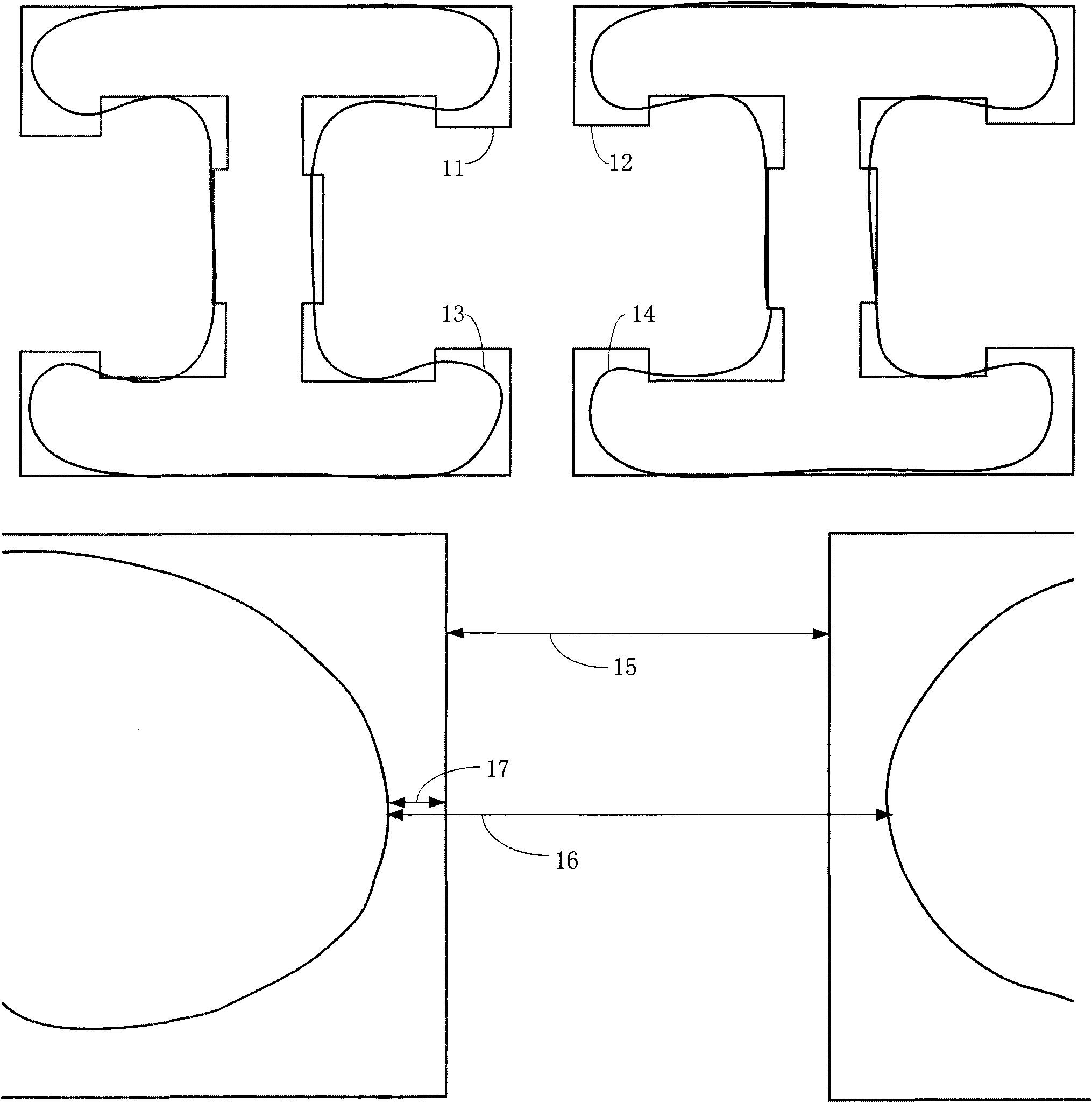
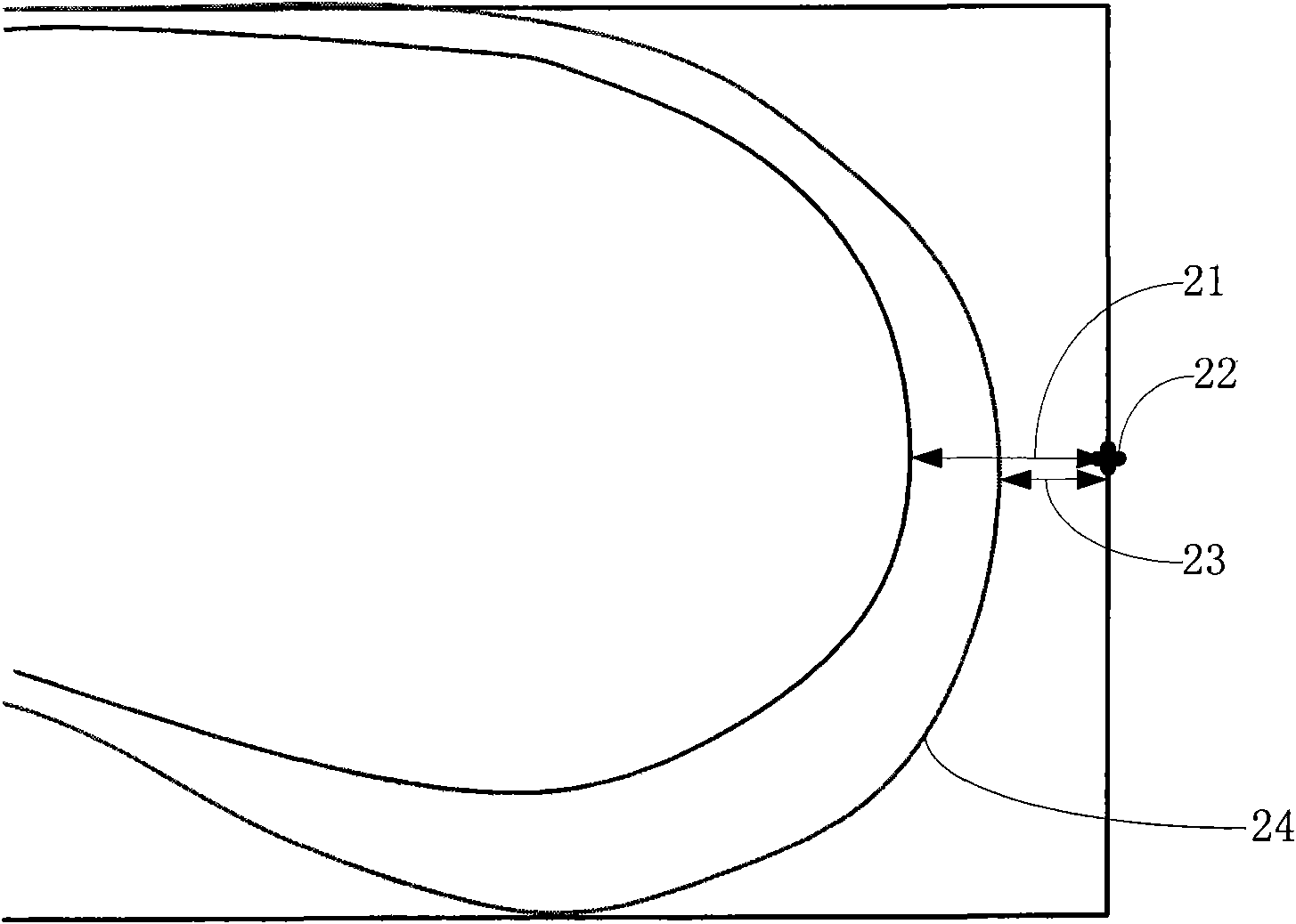
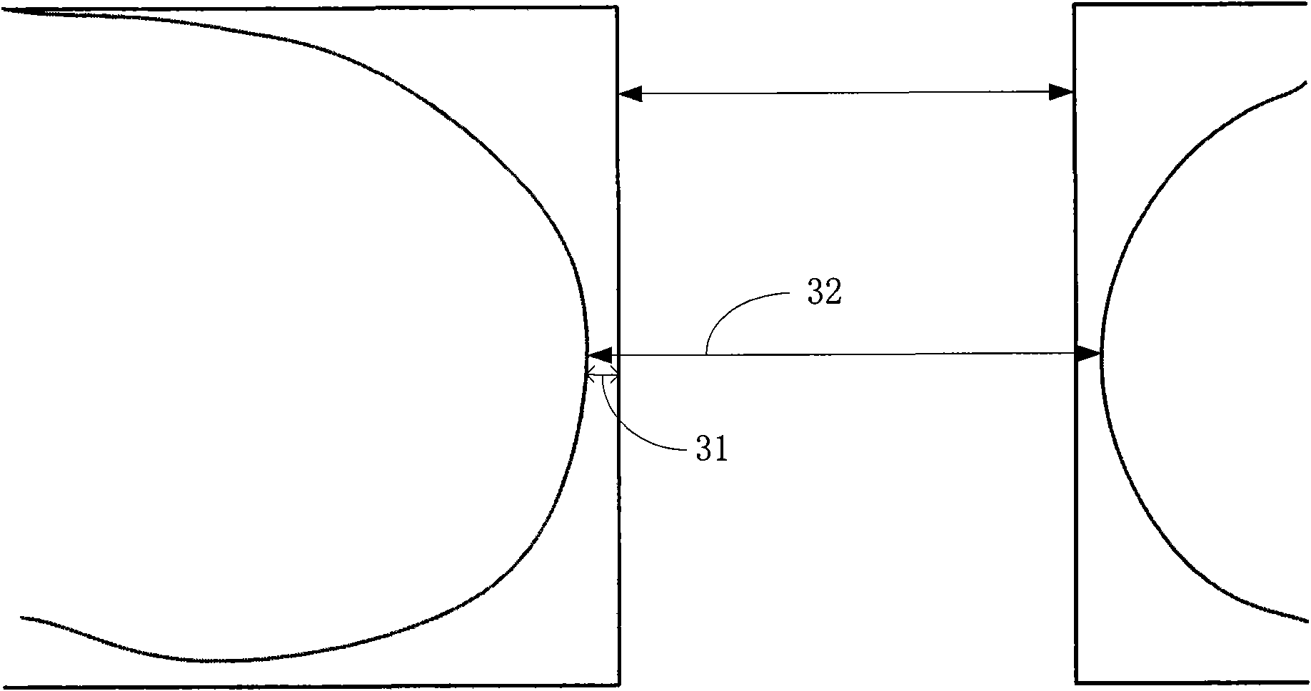
[0028] Establish a two-dimensional design graphic, and set the edge placement error of key dimensions that need to be compensated;

[0029] On the design graphic, first select a point (usually the center of the design graphic side) as the first sampling point, then take the sampling point at a predetermined interval (preferably 30nm) to divide the design graphic with the first sampling point;

[0030] Use the optical proximity correction technique for correction and simulation to obtain the edge placement errors of all sampling points;

[0031] A standard optical proximity correction model is est...


PUM


Abstract

The invention relates to a method for compensating deformation effect after exposure of a two-dimensional design layout. The method comprises the following steps of: establishing the two-dimensional design layout, and setting a key size edge placement error to be compensated; selecting a point on the design layout as a first sampling point, and then selecting sampling points at predetermined intervals from the first sampling point to partition the design layout; performing corrosion and simulation by using optical approaching correction technology to acquire edge placement errors of the points; and establishing a standard optical approaching correction model, and selecting the acquired point, the edge placement error of which is closest to the key size edge placement error, as a calculation point of the compensated edge placement error. The method saves repair of a design layout checking routine, greatly reduces time consumption, shortens the correction period, reduces the workload, and improves the accuracy.

Description

【Technical field】 [0001] The invention relates to a compensation method for a semiconductor lithography process, in particular to a compensation method for the deformation effect of a two-dimensional design pattern after exposure in the semiconductor lithography process. 【Background technique】 [0002] In the traditional 0.13-node photolithography process, the head-to-head line-end short effect of the two-dimensional design pattern (layout) is very serious, and the unilateral shortening (short) may reach 25nm ~ 30nm. Moreover, the tightening of straight ends of two-dimensional design figures of different shapes is also different. [0003] figure 1 is a schematic illustration of a typical end-of-line crunch effect for 2D design graphics. figure 1 Frames 11 and 12 in the above figure are chip design graphics, and areas 13 and 14 are graphics after the design graphics are exposed on the silicon wafer. figure 1 The lower image is a partial enlargement of the upper image. Th...

Claims


Application Information

Patent Timeline
IPC IPC(8): G03F1/00G03F1/36
Inventor 黄旭鑫王瑾恒
Owner WUXI DISI MICROELECTRONICS CO LTD
Why Eureka
Try Eureka