
Dynamic random access memory (DRAM)

A memory and storage unit technology, applied in the field of memory, can solve problems such as multi-storage unit area, low noise immunity, and DRAM memory process difficulties, and achieve the effect of reducing free area, low noise immunity, and good use of storage unit area

Inactive Publication Date: 2011-05-11
SEMICON MFG INT (SHANGHAI) CORP +1
View PDF0 Cites 3 Cited by
  • Summary
  • Abstract
  • Description
  • Claims
  • Application Information

AI Technical Summary

Problems solved by technology

[0008] The problem to be solved by the present invention is to provide a kind of DRAM memory, to solve the existing 2 memory cell DRAM memory consumes more memory cell area, and the existing 6F 2 The DRAM memory of the storage unit adopts the difficulty in the process of using a smaller storage unit, and uses an open folded bit line structure, which leads to the disadvantages of low noise immunity and reduced signal-to-noise ratio

Method used


Image

  • Dynamic random access memory (DRAM)
  • Dynamic random access memory (DRAM)
  • Dynamic random access memory (DRAM)

Examples


Embodiment Construction

[0029] The DRAM memory provided by the present invention has 7F 2 Storage unit, where F represents the feature size (featue size), 7F 2 Indicates the area of ​​each storage unit. The DRAM memory of the present invention will be described in detail below with reference to the accompanying drawings.

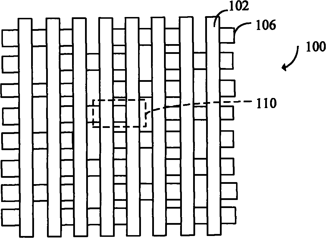
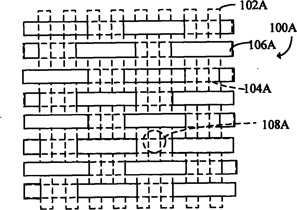
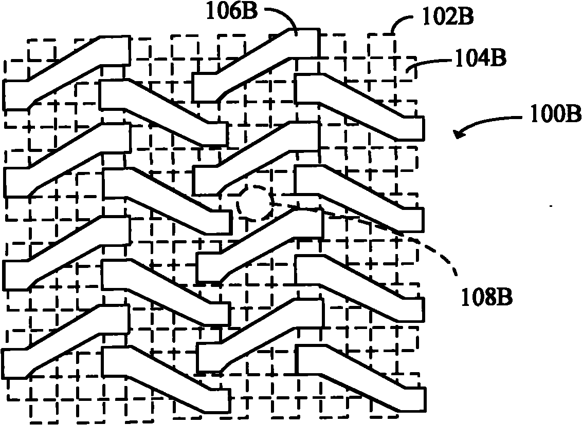
[0030] refer to image 3 It is a schematic diagram of the local layout of the DRAM memory of a specific embodiment of the present invention, while referring to Figure 4 for image 3 A partial layout diagram of the shown DRAM memory showing the location of the active area. The memory 300 includes a plurality of memory cells 302, an active area 304, word lines 306 arranged in parallel and equally spaced, and bit lines 308 arranged in parallel and equally spaced and perpendicular to the word lines. Wherein, the area of ​​each storage unit 302 is 7F 2 ; The pitch Lw between the word lines 306 is 2F, and the pitch Lb between the bit lines 308 is The storage unit area (cell_size...


PUM


Abstract

The invention provides a dynamic random access memory (DRAM), which comprises a memory unit with an area of 7F2, parallel word lines arranged at equal intervals and parallel bit lines which are arranged at equal intervals and vertical to the word lines, wherein the pitch between the word lines is 2F; the pitch between the bit lines also comprises a plurality of active areas; the connecting lines between the center of each active area and the centers of two adjacent active areas which are on the same adjacent bit line forms an equilateral triangle, and the length of the edge of the equilateral triangle is 4F. When the technical scheme is implemented, the memory unit area can be better used by adopting the memory unit with an area of 7F2 as a folding bit line memory unit than adopting the memory unit with an area of 8F2 as the folding bit line memory unit; and compared with a DRAM having the memory unit with an area of 6F2, the DRAM having the memory unit with the area of 7F2 does not have technical difficulties, and drawbacks of low noise immunity and low signal to noise ratio, which are caused by an open bit line structure, of the DRAM having the memory unit with the area of 6F2.

Description

technical field [0001] The invention relates to a memory, in particular to a DRAM memory. Background technique [0002] Integrated circuits have evolved from integrating dozens of devices on a single chip to integrating millions of devices. The performance and complexity of traditional integrated circuits have far exceeded the original imagination. To achieve increases in complexity and circuit density (the number of devices that can fit on a given chip area), the feature size of a device, also called "geometry," has grown with each generation of integrated circuits Getting smaller and smaller. Increasing integrated circuit density not only increases the complexity and performance of integrated circuits, but also reduces costs for consumers. Making devices smaller is challenging because every process in integrated circuit manufacturing has a limit, that is, if a certain process is to be performed under the condition of being smaller than the feature size, the process or d...

Claims


Application Information

Patent Timeline
Patent Type & Authority Applications(China)
IPC IPC(8): G11C11/4097
CPCH01L27/0207H10B12/482
Inventor 邢溯杨勇胜肖德元陈国庆
Owner SEMICON MFG INT (SHANGHAI) CORP
Learn More