Static discharge test method

A technology of electrostatic discharge test and test board, which is applied in the direction of single semiconductor device test, etc., can solve the problems of quantity limitation, time-consuming, cost increase, etc., and achieve the effect of saving time and reducing cost

Inactive Publication Date: 2011-05-11
SEMICON MFG INT (SHANGHAI) CORP +1
View PDF0 Cites 3 Cited by
  • Summary
  • Abstract
  • Description
  • Claims
  • Application Information

AI Technical Summary

Problems solved by technology

[0009] The purpose of the present invention is to provide an electrostatic discharge test method, which solves the problems in the prior art that the number of contact points of the semiconductor device to be tested is limited, and a special test board must be additionally reconfigured, resulting in time-consuming and cost-increasing problems.

Method used


Image

  • Static discharge test method
  • Static discharge test method
  • Static discharge test method

Examples


Embodiment Construction

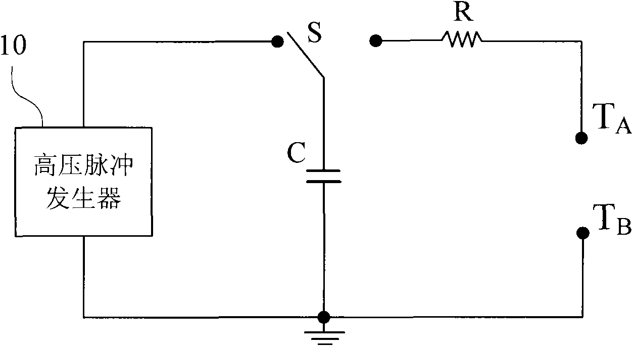
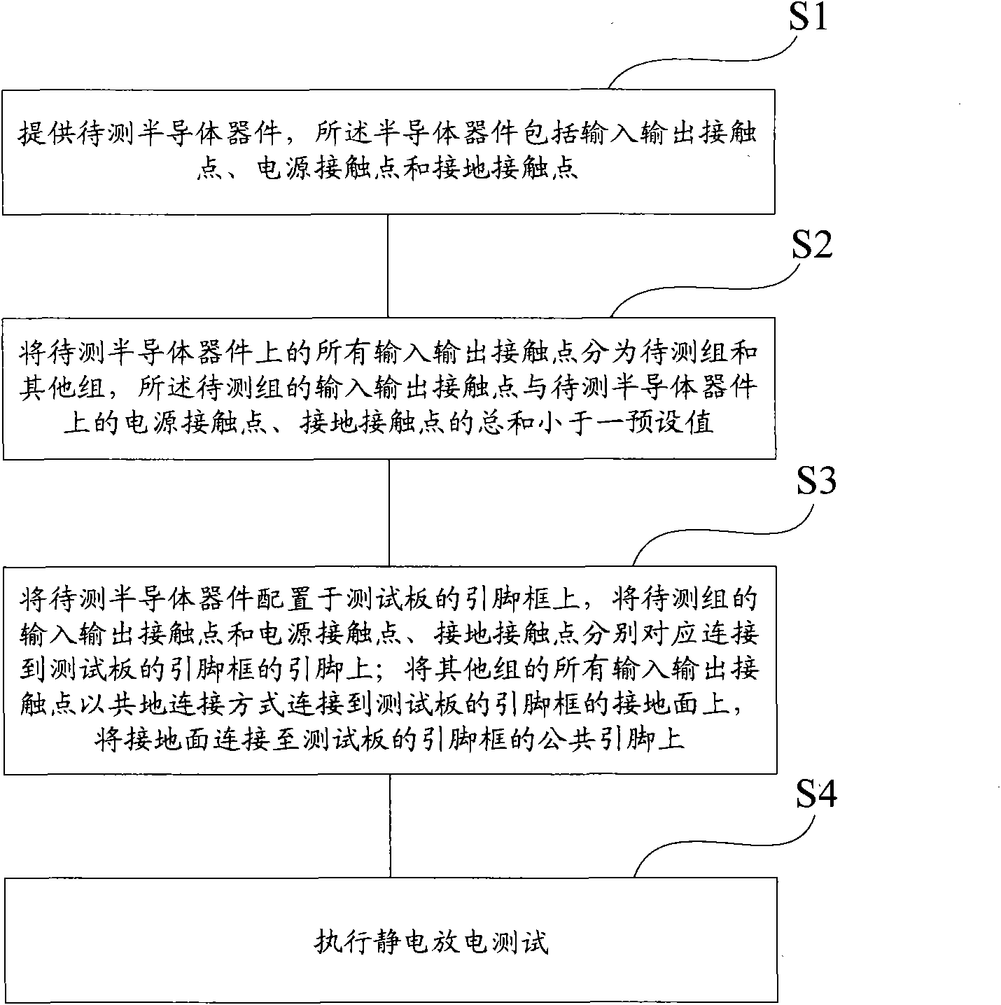
[0023] The inventors have found that with the development of semiconductor technology, the integration of semiconductor devices is getting higher and higher, and there are more and more contact points on the semiconductor device, so that the number of pins on the original test board is smaller than the contact points of the semiconductor device The quantity, can not use the traditional electrostatic discharge test method to test on the test board.

[0024] In order to solve the contradiction in quantity between the pins on the existing test board and the contact points of the semiconductor device to be tested, in view of this, the inventor of the present invention provides a kind of electrostatic discharge test especially for the semiconductor device with many contact points method.

[0025] refer to figure 2 , the embodiment of the present invention provides an electrostatic discharge test method, including:

[0026] Step S1 is executed to provide a semiconductor device to...


PUM


Abstract

The invention provides a static discharge test method, comprising the following steps of: providing a semiconductor device to be tested; dividing all input and output contacts which are disposed on the semiconductor device to be tested into a standby group and other groups; placing the semiconductor device to be tested on a pin frame of a test plate which is provided, wherein the input and output contacts of the a standby group and a power supply contact and a grounding contact of the semiconductor device to be tested are respectively and correspondingly connected to the pin of the pin frame of the test plate; then connecting all input and output contacts of other groups to a grounding plane of the pin frame of the test plate by means of common ground connection, and connecting the grounding plane to a common pin of the pin frame of the test plate; and then implementing the static discharge test. The static discharge test method provided by the invention has the advantages that the limitation to the contact amount of the semiconductor device to be tested in the prior art is solved without influencing the results of the test by means of the strategy of grouping, the time is saved, and the cost is reduced.

Description

technical field [0001] The invention relates to electrostatic discharge testing technology, in particular to an electrostatic discharge testing method for semiconductor devices. Background technique [0002] Electrostatic discharge (Electro Static Discharge; ESD) refers to the transfer of electrostatic charges between objects caused by direct contact or electrostatic induction of objects with different electrostatic potentials. It usually refers to the phenomenon that after the energy of the electrostatic field reaches a certain level, it breaks down the medium and discharges it. The instantaneous voltage generated when electrostatic discharge occurs can be as high as thousands of volts, which usually generates enough heat to melt the working circuit inside the semiconductor, causing immediate and irreversible damage, which we try our best to avoid. [0003] Therefore, ESD testing is required for semiconductor devices. [0004] At present, ESD is mainly divided into three ...

Claims


Application Information

Patent Timeline
Patent Type & Authority Applications(China)
IPC IPC(8): G01R31/26
Inventor 冯军宏简维廷张荣哲
Owner SEMICON MFG INT (SHANGHAI) CORP
Why Eureka
Try Eureka