
Method for preparing counterfeit antiferroelectric film

A ferroelectric thin film and antiferroelectric technology, applied in the field of microelectronics, can solve the problems of different processes and material components, limitations of antiferroelectric thin films, etc.

Inactive Publication Date: 2011-04-06
FUDAN UNIV
View PDF0 Cites 2 Cited by
  • Summary
  • Abstract
  • Description
  • Claims
  • Application Information

AI Technical Summary

Problems solved by technology

[0002] The main value of antiferroelectric thin films is that they can be used in the field of high charge density storage devices, but the preparation of antiferroelectric thin films is limited by the types of inherent antiferroelectric materials. different material components

Method used


Image

  • Method for preparing counterfeit antiferroelectric film
  • Method for preparing counterfeit antiferroelectric film
  • Method for preparing counterfeit antiferroelectric film

Examples


Embodiment Construction

[0029] Hereinafter, the present invention is described more specifically in reference examples with reference to the drawings, and the present invention provides preferred embodiments, but should not be construed as being limited to the embodiments set forth herein. In the drawings, the thicknesses of layers and regions are exaggerated for convenience of illustration, and the shown sizes do not represent actual sizes.

[0030] The referenced figures are schematic illustrations of idealized embodiments of the invention, and the illustrated embodiments of the invention should not be construed as limited to the particular shapes of regions illustrated in the figures but are to include resulting shapes, such as manufacturing-induced deviations. For example, the curves obtained by etching are usually curved or rounded, but in the embodiment of the present invention, they are all represented by rectangles. The representation in the figure is schematic, but this should not be consider...


PUM


Abstract

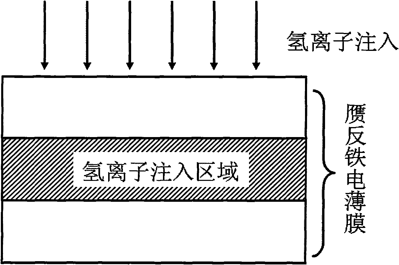
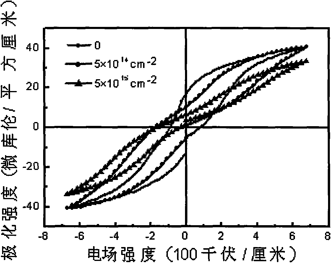
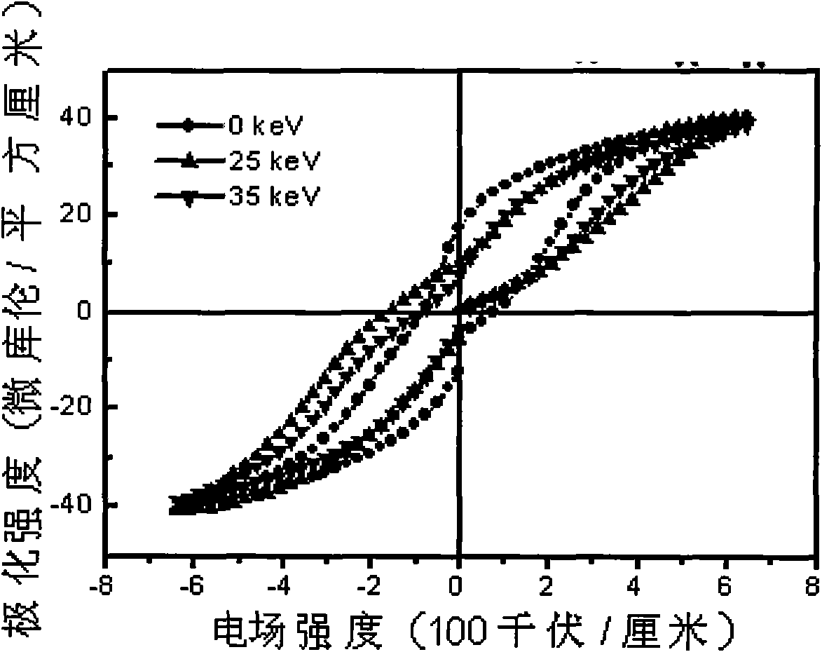
The invention relates to a method for preparing a counterfeit antiferroelectric film, belonging to the technical field of micro-electronics. In the preparation method, stably distributed doping ions are formed in a ferroelectric film by injecting and doping a certain dose of hydrogen ions with certain energy, and the overturning characteristic of a ferroelectric film domain is changed through a charge compensation mode. The preparation method can realize the antiferroelectric characteristic of the ferroelectric film in the ferroelectric film with any component proportion and can be applied to the field of storage of high-density charges. The invention not only provides a new preparation method of the counterfeit antiferroelectric film, but also is beneficial to further intensive study on the overturning physical mechanism of the electric domain of the ferroelectric film, and has great academic significance.

Description

technical field [0001] The invention belongs to the technical field of microelectronics, and in particular relates to a preparation method of a pseudo-antiferroelectric thin film. Background technique [0002] The main value of antiferroelectric thin films is that they can be used in the field of high charge density storage devices, but the preparation of antiferroelectric thin films is limited by the types of inherent antiferroelectric materials. The material composition is different. The choice of material components of antiferroelectric thin films is very small. For example, in PZT, the ratio of zirconium (Zr) to titanium (Ti) can only be between 95:5 and 99:1. Once this range is exceeded, iron Electric thin films do not show antiferroelectric properties. Contents of the invention [0003] The purpose of the present invention is to overcome the deficiencies in the prior art, to propose a new preparation method for pseudo-antiferroelectric thin films, to realize the an...

Claims


Application Information

Patent Timeline
Patent Type & Authority Applications(China)
IPC IPC(8): H01L21/314H01L21/3105H01L27/10
Inventor 翁旭东万海军张燕均张鑫江安全
Owner FUDAN UNIV
Learn More