Semiconductor device and method for manufacturing the same

A device manufacturing method and semiconductor technology, applied in semiconductor/solid-state device manufacturing, semiconductor devices, semiconductor/solid-state device components, etc., can solve the problems of metal plug short circuit, shrinkage, position dislocation, etc., to reduce the circuit area, less The effect of restriction

Active Publication Date: 2011-03-30
SONY GRP CORP
View PDF4 Cites 17 Cited by
  • Summary
  • Abstract
  • Description
  • Claims
  • Application Information

AI Technical Summary

Problems solved by technology

[0008] In the technique disclosed in Japanese Patent Application JP-A-2001-291770, since the contact plug and the control electrode are separated only by the first side wall spacer, there is a high possibility of a short circuit between the contact plug and the control electrode
In addition, since the contact plug is formed in the form of a side wall, position misregistration is likely to occur between the contact plug and the metal plug connected thereto.
In addition, when the width of the element isolation region is made narrow due to the miniaturization of the circuit, since the distance between the metal plug and the metal plug connected to the contact plug disposed near the element isolation region is shortened, there is a high possibility of a gap between the metal plugs. short circuit
For this reason, the technology disclosed in the Japanese patent application JP-A-2001-291770 is not suitable for the miniaturization process, and it is difficult to reduce the circuit area by this technology

Method used


Image

  • Semiconductor device and method for manufacturing the same
  • Semiconductor device and method for manufacturing the same
  • Semiconductor device and method for manufacturing the same

Examples


Embodiment 1

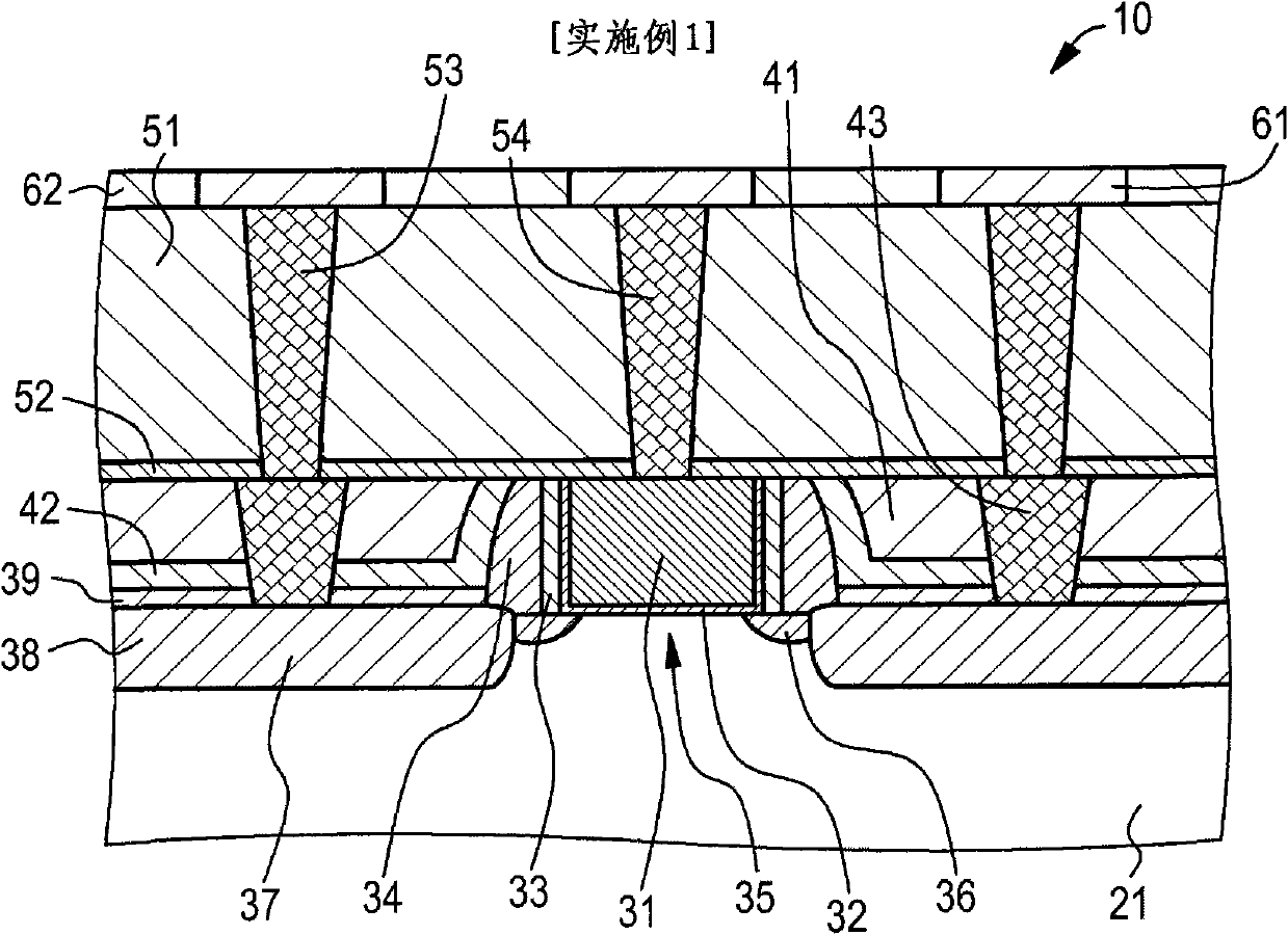
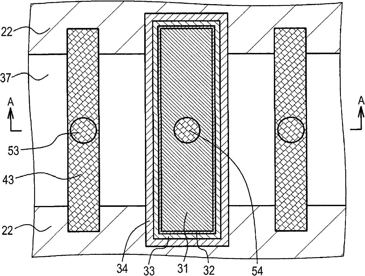
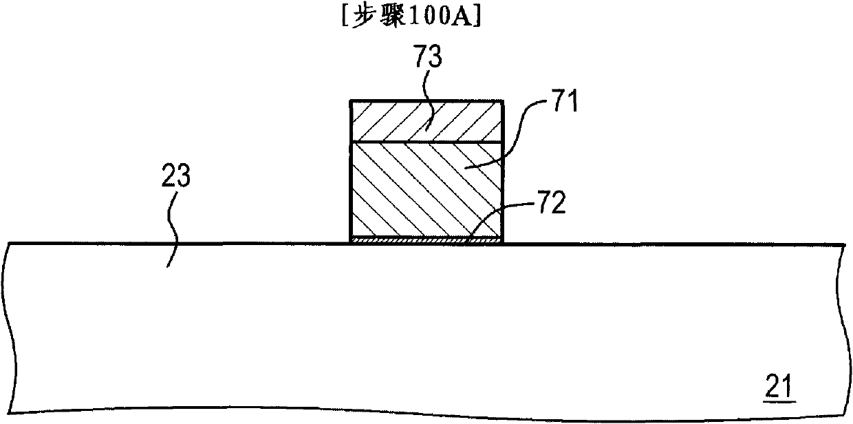
[0043] 2. Example 1 (semiconductor device and semiconductor device manufacturing method according to the first embodiment of the present invention)

Embodiment 2

[0044] 3. Embodiment 2 (modified example of embodiment 1)

Embodiment 3

[0045] 4. Example 3 (semiconductor device and semiconductor device manufacturing method according to the second embodiment of the present invention)

[0046] 5. Embodiment 4 (modified example of embodiment 3, and others)

[0047] 1. General description of semiconductor device and semiconductor device manufacturing method of the present invention

[0048] The semiconductor device or semiconductor device manufacturing method of the first embodiment of the present invention may be suitable for an n-channel semiconductor device or for providing an n-channel semiconductor device in which the first contact portion has tensile stress. Alternatively, the semiconductor device or the manufacturing method of the semiconductor device according to the first embodiment of the present invention may be suitable for a p-channel semiconductor device or for providing a p-channel semiconductor device in which the first contact portion with compressive stress.

[0049] In the semiconductor dev...


PUM


Abstract

The invention discloses a semiconductor device and a method for manufacturing the same. The method for manufacturing a semiconductor device includes the steps of: (a) forming a gate electrode on a substrate, forming source / drain regions and a channel forming region in the substrate, and forming on the source / drain regions a first interlayer insulating layer equal in height to the gate electrode; (b) forming in the first interlayer insulating layer groove-shaped first contact portions connected to the source / drain regions; (c) forming a second interlayer insulating layer on a whole surface; (d) forming hole-shaped second contact portions in portions of the second interlayer insulating layer on the first contact portion; and (e) forming on the second interlayer insulating layer wires connected to the second contact portions.

Description

[0001] Cross References to Related Applications [0002] This application contains subject matter related to that disclosed in Japanese Priority Patent Application JP2009-190645 filed with Japan Patent Office on Aug. 20, 2009, the entire content of which is hereby incorporated by reference incorporated into this article. technical field [0003] The invention relates to a semiconductor device and a method for manufacturing the semiconductor device. Background technique [0004] Recently, the trend toward miniaturization of components in semiconductor devices and semiconductor integrated circuits has caused a problem of increasing contact resistance. Meanwhile, many attempts have been made to improve the characteristics of circuit transistors using a technique aimed at increasing carrier mobility by applying stress to a channel formation region with a stressing material. [0005] Regarding the problem of increased contact resistance, for example, C.Auth et al. in "45nm High...

Claims


Application Information

Patent Timeline
Patent Type & Authority Applications(China)
IPC IPC(8): H01L21/28H01L29/41H01L29/417
CPCH01L21/823871H01L21/76897H01L23/485H01L21/76816H01L29/66636H01L2924/0002H01L21/2855H01L29/7834H01L21/76877H01L29/7845H01L21/28518H01L29/66545H01L27/092H01L21/76895H01L23/5226H01L21/76834H01L2924/00
Inventor 黛哲
Owner SONY GRP CORP
Why Eureka
Try Eureka