Heating device, substrate processing apparatus, and method of manufacturing semiconductor device
A technology for heating devices and substrates, which is used in the manufacture of semiconductor/solid-state devices, electrical components, circuits, etc., can solve problems such as component damage, and achieve the effects of reducing damage, inhibiting offset, and inhibiting shearing
- Summary
- Abstract
- Description
- Claims
- Application Information
AI Technical Summary
Problems solved by technology
Method used
Image

Examples
no. 1 approach
[0069] Next, a first embodiment of the present invention will be described with reference to the drawings.
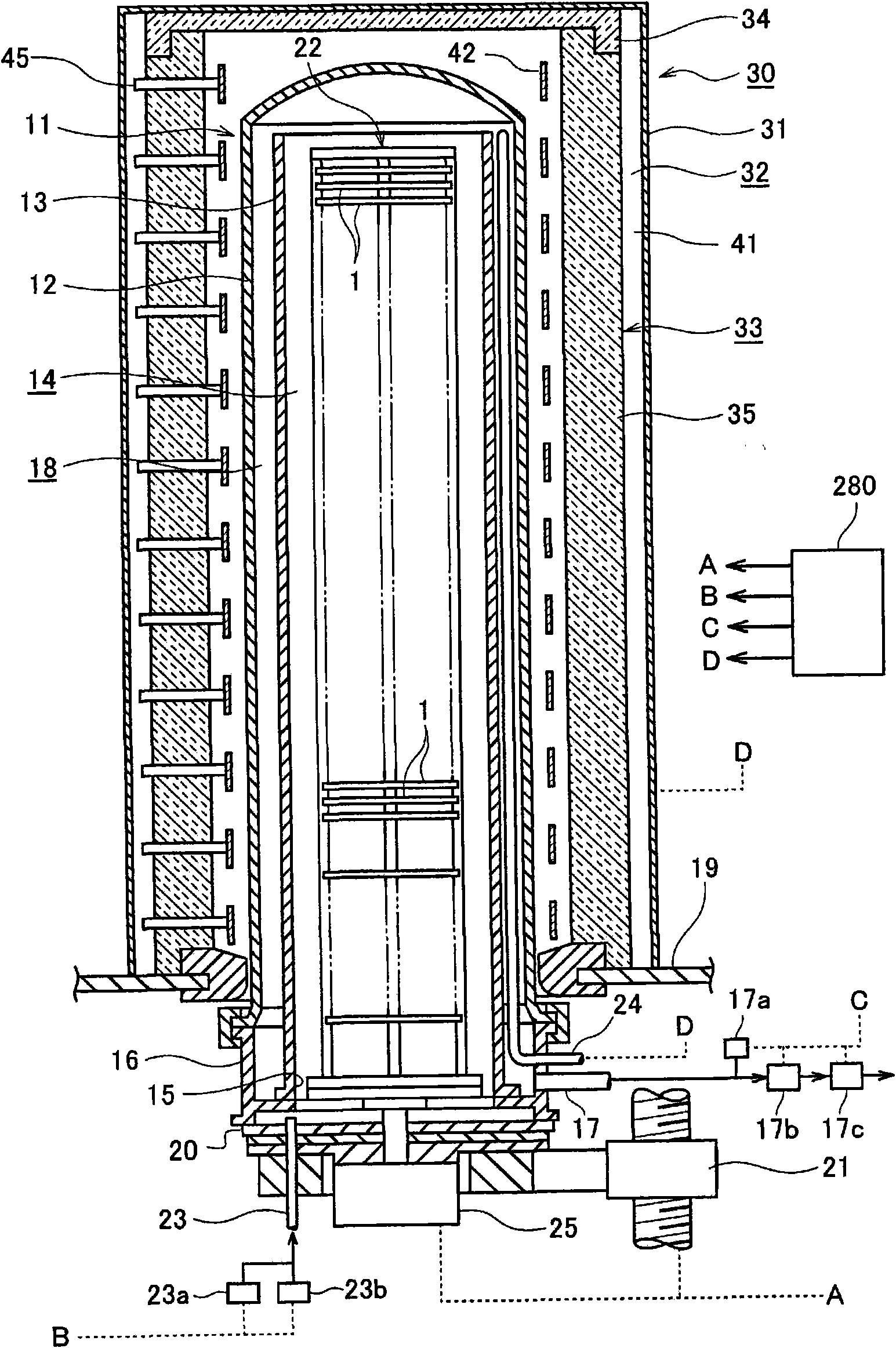
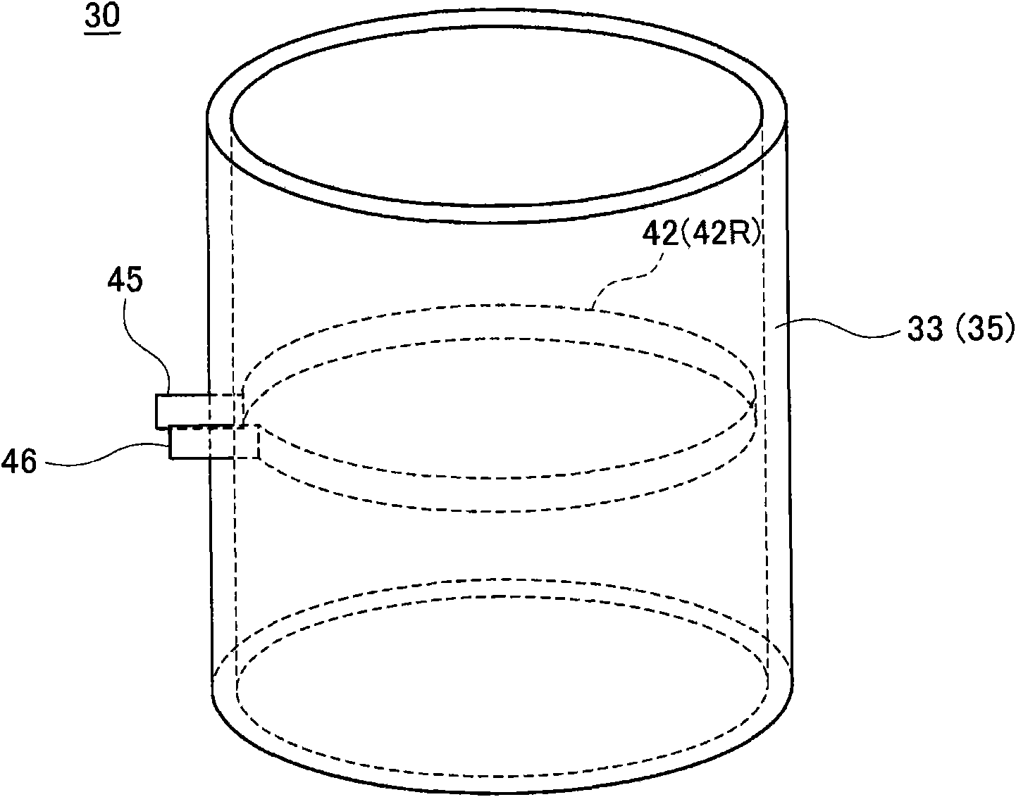
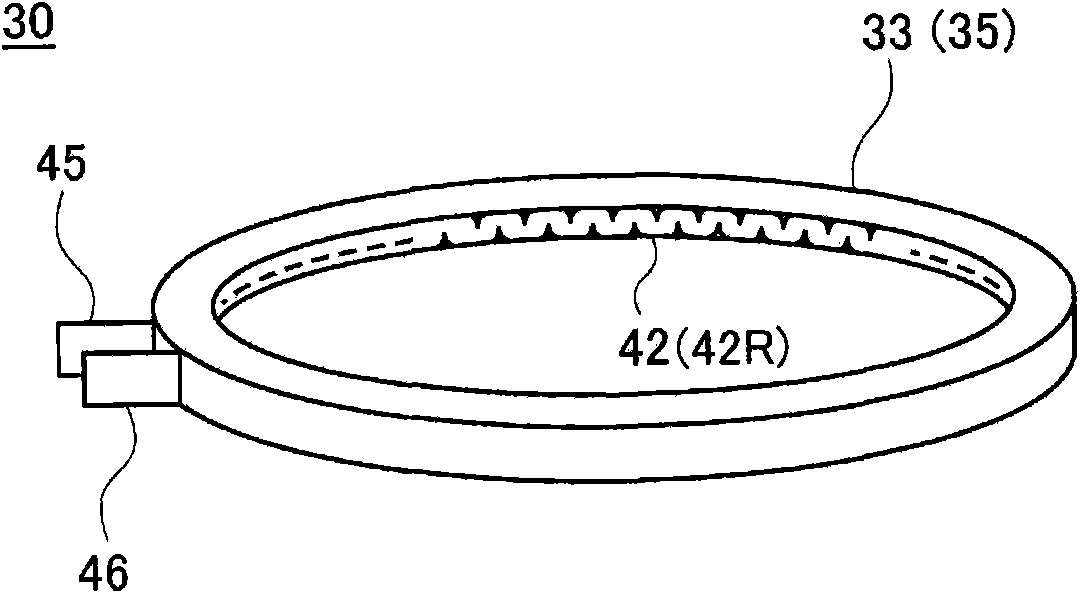
[0070] figure 1 is a vertical cross-sectional view showing the substrate processing apparatus according to the first embodiment of the present invention. figure 2 It is a perspective view of the heating unit of 1st Embodiment of this invention. image 3 It is a partially enlarged view of the heating unit according to the first embodiment of the present invention. Figure 4 (a) is a schematic diagram illustrating a linear material constituting an annular portion according to the first embodiment of the present invention, Figure 4 (b) is a schematic diagram illustrating an example of a plate-shaped material constituting the annular portion. Figure 19 (a) is a partial enlarged view of the annular portion of the first embodiment of the present invention, Figure 19 (b) is a side view of an enlarged part.
[0071] (1) Structure of the substrate processing device
[...
no. 2 approach
[0151] Next, a second embodiment of the present invention will be described with reference to the drawings.
[0152] Figure 25 is a vertical cross-sectional view showing a substrate processing apparatus according to a second embodiment of the present invention. Figure 26 It is a perspective view of the heating element of 2nd Embodiment of this invention. Figure 27 (a) is a partially enlarged view of an annular portion according to a second embodiment of the present invention, Figure 27 (b) is a side view of an enlarged part. Figure 28 It is a partial enlarged view of the heat insulator holding the annular part of the second embodiment of the present invention, Figure 28 (a) represents the situation before warming, Figure 28 (b) shows the situation after temperature rise.
[0153] (1) Composition of heating element and heat insulator
[0154] The substrate processing apparatus of this embodiment is different from the above-mentioned embodiment in the configuration of...
no. 3 approach
[0169] Next, a third embodiment of the present invention will be described with reference to the drawings.
[0170] Figure 6 It is a horizontal cross-sectional view of the heating unit 30 before temperature rise according to the third embodiment of the present invention. Figure 7 It is a horizontal cross-sectional view of the heated heating unit 30 according to the third embodiment of the present invention.
[0171] In the substrate processing apparatus of this embodiment, if Figure 6 As shown, the distance between the bottom surface 40e and the central portion 42e is set so that at least when the annular portion 42R is in a room temperature state, it becomes larger as the distance from the pair of power supply portions 45, 46 increases (that is, it is set in a room temperature state). When it becomes A Figure 7 As shown, the distance between the bottom surface 40e and the central portion 42e is set so that, at least when the annular portion 42R is in the temperature stat...
PUM
 Abstract
Description
Claims
Application Information
 - Generate Ideas
- Intellectual Property
- Life Sciences
- Materials
- Tech Scout
- Unparalleled Data Quality
- Higher Quality Content
- 60% Fewer Hallucinations
Browse by: Latest US Patents, China's latest patents, Technical Efficacy Thesaurus, Application Domain, Technology Topic, Popular Technical Reports.
© 2025 PatSnap. All rights reserved.Legal|Privacy policy|Modern Slavery Act Transparency Statement|Sitemap|About US| Contact US: help@patsnap.com