


Quick Research
Generate reliable direction feasibility study reports for your R&D in just a few steps.

Technical Q&A
Discover and master advanced knowledge NOW. Basics, ideas, possibilities, all at once.

Find Solutions
As an expert in R&D theories, this can generate solutions to your technical problems instantly.

Evaluate Feasibility
Analyze your overall solution with one click, know your potential R&D risks in advance.

Monitor Landscape
Get weekly tech updates, stay abreast of the latest tech innovations and key insights.
Method for preparing copper indium gallium selenide film and photovoltaic film battery based on selenium plasma
A technology of photovoltaic thin film and copper indium gallium selenide, which is applied in the field of copper indium gallium selenide photovoltaic thin film preparation by ions, can solve the problems of high substrate temperature and impossibility of depositing copper indium gallium selenide thin film, so as to reduce the selenization temperature and material The effect of high scale accuracy
- Summary
- Abstract
- Description
- Claims
- Application Information
AI Technical Summary
Problems solved by technology
Method used
Image

Examples
example 1
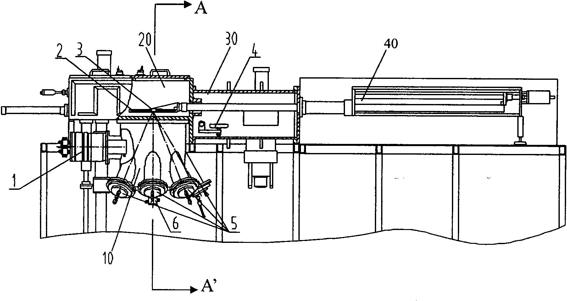
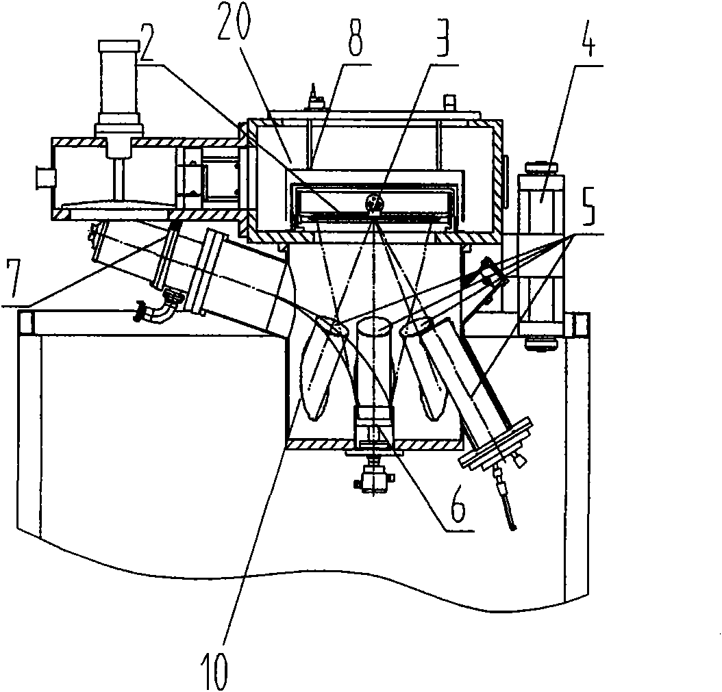
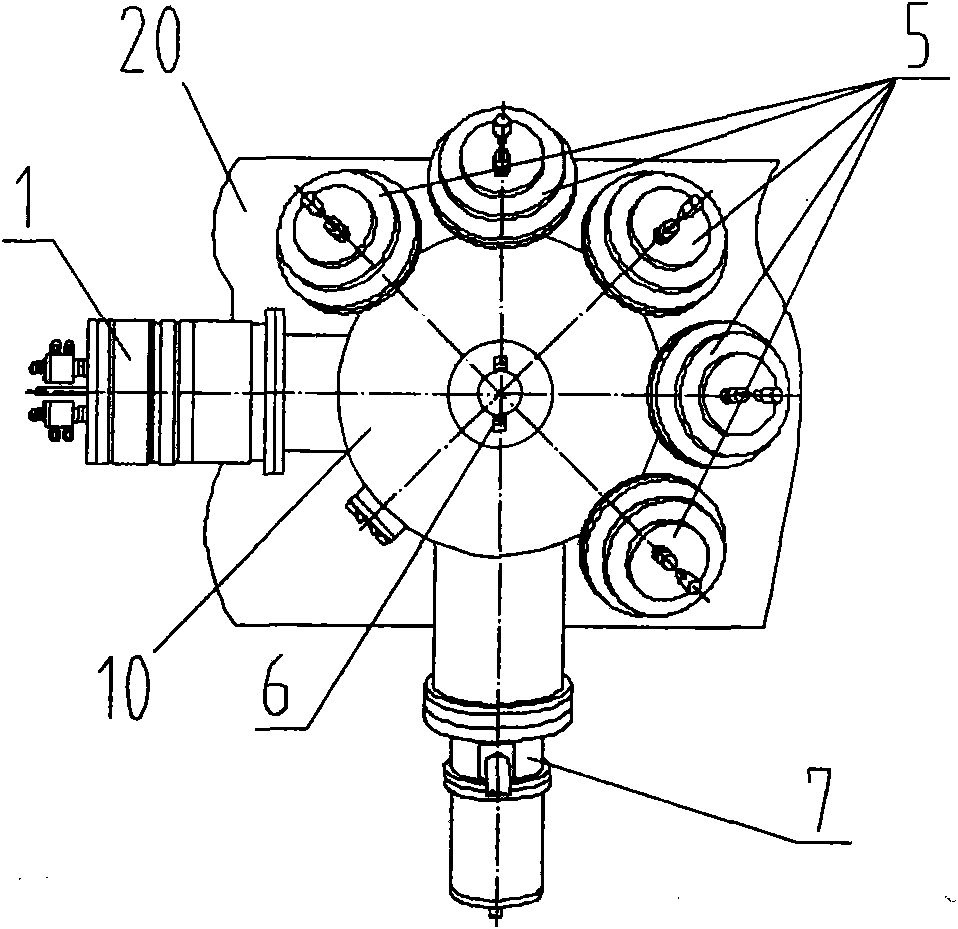
[0062] In the present invention, the evaporation source chamber, film deposition chamber, and transition chamber are evacuated to 8×10 -4 Pa, turn on the baking system in the thin film deposition chamber, heat to 300°C, turn on the substrate holder heater to heat the substrate at a heating temperature of 350°C, and then introduce Ar gas through the gas inlet of the high-current ion source, and maintain the vacuum at 1× 10 -2 Pa, turn on the suspension bias electron gun, the crucible bias is 120V, turn on the high-current ion source, the discharge current is 60A, maintain the normal discharge of the high-current ion source, turn on the suspension bias electron gun, the acceleration voltage is DC-6KV; the beam current is 0.5A, for The selenium material is evaporated to produce selenium vapor, and the suspension crucible is connected to positive bias, so that the electron cloud generated by the working gas in the ionization process collides with the selenium vapor under the actio...
example 2
[0067] Vacuum the evaporation source chamber, thin film deposition chamber, and transition chamber to 8×10 -4 Pa, turn on the baking system in the film deposition chamber, heat to 350°C, turn on the substrate holder heater to heat the substrate at a heating temperature of 490°C, and then introduce Ar gas through the gas charging port of the high-current ion source, and maintain the vacuum at 1× 10 -2 Pa, turn on the suspension bias electron gun with a crucible bias of 150V, turn on the high-current ion source, and discharge the current at 70A, maintain the normal discharge of the high-current ion source, turn on the suspension bias electron gun, and accelerate the voltage DC-6KV; the beam current is 0.4A for The selenium material is evaporated to produce selenium vapor, and the suspension crucible is connected to positive bias, so that the electron cloud generated by the working gas in the ionization process collides with the selenium vapor under the action of the suspension c...
example 3
[0069] In the present invention, the evaporation source chamber, film deposition chamber, and transition chamber are evacuated to 8×10 -4 Pa, turn on the baking system in the film deposition chamber, heat to 50°C, turn on the substrate holder heater to heat the substrate at a heating temperature of 25°C, and then introduce Ar gas through the gas charging port of the strong current ion source, and maintain the vacuum at 2× 10 -2 Pa, turn on the suspension bias electron gun, the crucible bias is 120V, turn on the high-current ion source, the discharge current is 100A, maintain the normal discharge of the high-current ion source, turn on the suspension bias electron gun, the acceleration voltage is DC-5KV; the beam current is 0.5A, for The selenium material is evaporated to produce selenium vapor, and the suspension crucible is connected to positive bias, so that the electron cloud generated by the working gas in the ionization process collides with the selenium vapor under the a...
PUM
 Abstract
Description
Claims
Application Information
 - R&D Engineer
- R&D Manager
- IP Professional
- Industry Leading Data Capabilities
- Powerful AI technology
- Patent DNA Extraction
Browse by: Latest US Patents, China's latest patents, Technical Efficacy Thesaurus, Application Domain, Technology Topic, Popular Technical Reports.
© 2024 PatSnap. All rights reserved.Legal|Privacy policy|Modern Slavery Act Transparency Statement|Sitemap|About US| Contact US: help@patsnap.com