Silicon on insulator (SOI) wafer double-mask etching-based vertical comb teeth driven torsional micro-mirror and manufacturing method thereof
A technology of vertical comb driving and micro-torsion mirror, which is applied in the photoplate making process of patterned surface, the process for producing decorative surface effects, microstructure technology, etc., which can solve the problem of large process error, high cost and complicated process steps and other issues, to achieve the effect of reducing process cost, increasing resonance frequency and increasing flexibility
- Summary
- Abstract
- Description
- Claims
- Application Information
AI Technical Summary
Problems solved by technology
Method used
Image
Examples
Embodiment 1
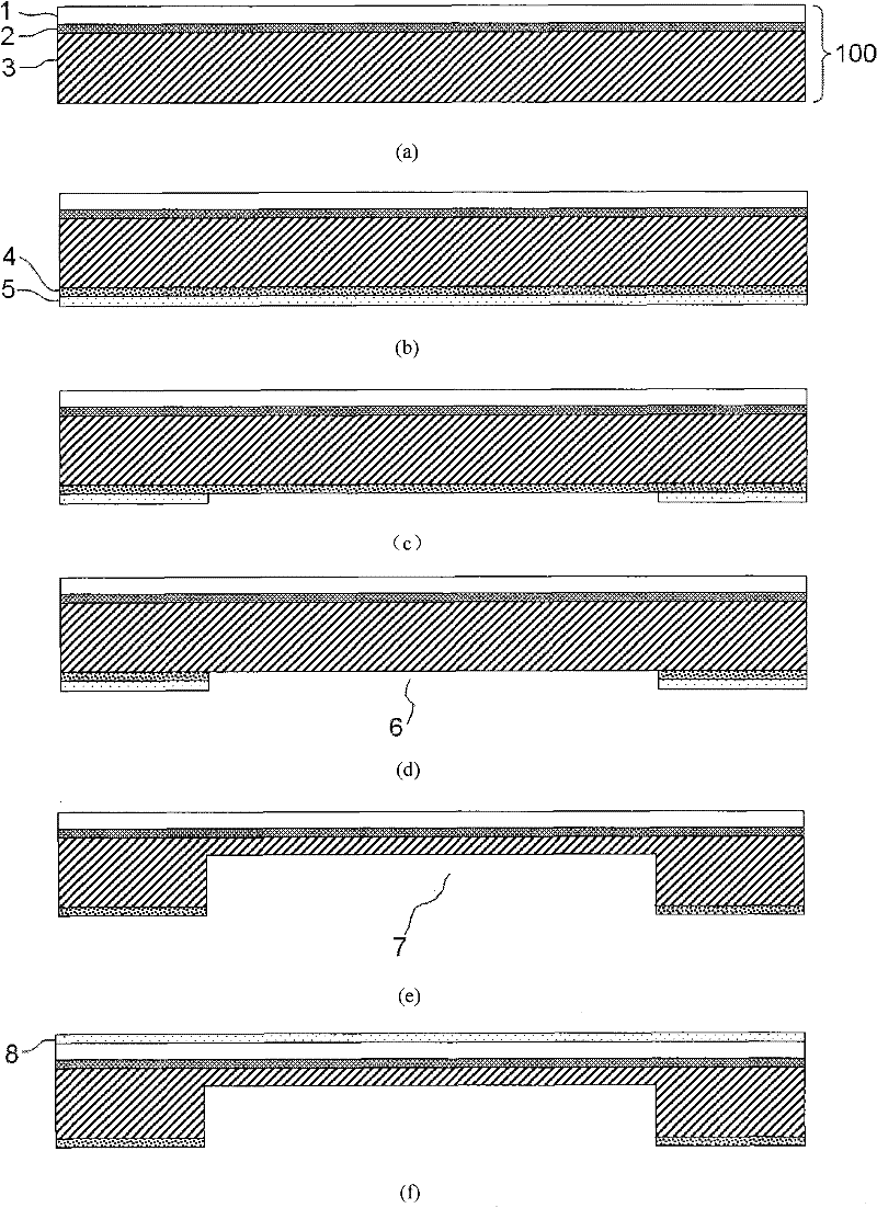
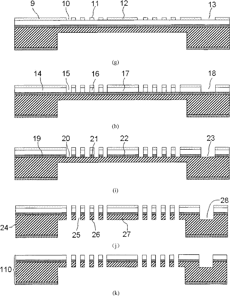
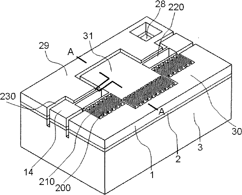
[0045] The vertical comb driven micro-torsion mirror based on SOI wafer double-mask etching in this embodiment sequentially includes a device layer 1, an insulating layer 2, and a base layer 3 with the same structure; the device layer 1 includes movable parts separated from each other and the fixed part, the movable part and the fixed part are separated by the device layer insulation groove 230, and the movable part is composed of the device layer mirror surface 31, the device layer torsion beam 220, the device layer anchor region 14 and the device layer movable comb teeth 210, The device layer mirror 31 is respectively connected to the device layer anchor regions 14 on both sides through the device layer torsion beams 220 at both ends. The movable comb 210; the fixed part is the part that is separated and arranged around the movable part, including the device layer without comb teeth anchor point 29, the device layer fixed comb tooth anchor point 30 and the device layer fixed ...
Embodiment 2
[0061] The vertical comb driven micro-torsion mirror based on SOI wafer double-mask etching in this embodiment sequentially includes a device layer 1, an insulating layer 2, and a base layer 3 with the same structure; the device layer 1 includes movable parts separated from each other and the fixed part, the movable part and the fixed part are separated by the device layer insulation groove 230, and the movable part is composed of the device layer mirror surface 31, the device layer torsion beam 220, the device layer anchor region 14 and the device layer movable comb teeth 210, The device layer mirror 31 is respectively connected to the device layer anchor regions 14 on both sides through the device layer torsion beams 220 at both ends. The movable comb 210; the fixed part is the part that is separated and arranged around the movable part, including the device layer without comb teeth anchor point 29, the device layer fixed comb tooth anchor point 30 and the device layer fixed ...
PUM
 Abstract
Description
Claims
Application Information
 - Generate Ideas
- Intellectual Property
- Life Sciences
- Materials
- Tech Scout
- Unparalleled Data Quality
- Higher Quality Content
- 60% Fewer Hallucinations
Browse by: Latest US Patents, China's latest patents, Technical Efficacy Thesaurus, Application Domain, Technology Topic, Popular Technical Reports.
© 2025 PatSnap. All rights reserved.Legal|Privacy policy|Modern Slavery Act Transparency Statement|Sitemap|About US| Contact US: help@patsnap.com


