Printed wiring board and manufacturing method of the same

A technology for printed circuit boards and substrates, applied in the directions of printed circuit manufacturing, printed circuits, printed circuit dielectrics, etc., can solve the problems of difficulty in simplifying the manufacturing process, complexity, and low adhesion of insulating substrates, and achieve the effect of realizing the manufacturing process.

Inactive Publication Date: 2010-11-17
HITACHI CABLE
View PDF4 Cites 6 Cited by
  • Summary
  • Abstract
  • Description
  • Claims
  • Application Information

AI Technical Summary

Problems solved by technology

[0012] In the past, generally, the manufacturing process of the additive method is more complicated than that of the subtractive method (subtractive), and there are problems that it is difficult to simplify the manufacturing process and reduce the cost. The problem of low adhesion of the substrate

Method used


Image

  • Printed wiring board and manufacturing method of the same
  • Printed wiring board and manufacturing method of the same
  • Printed wiring board and manufacturing method of the same

Examples


Embodiment

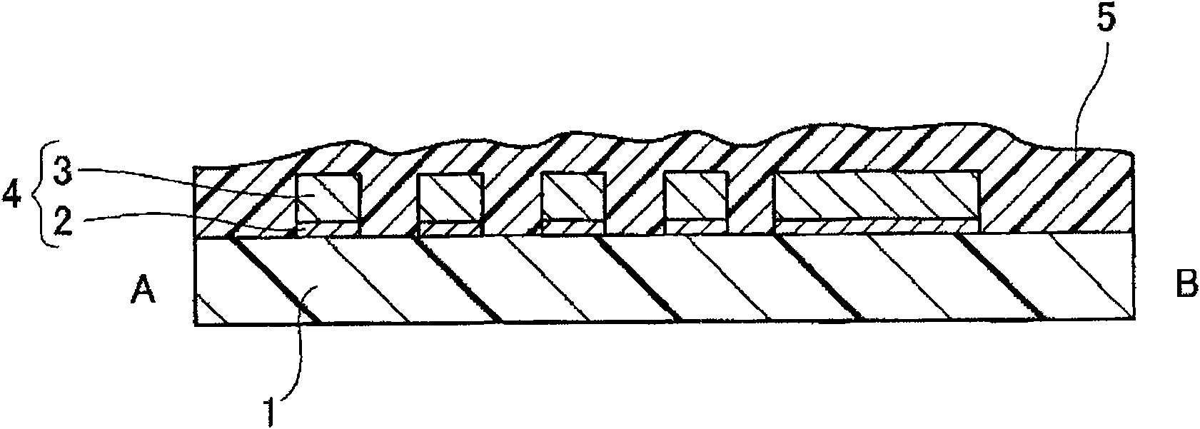
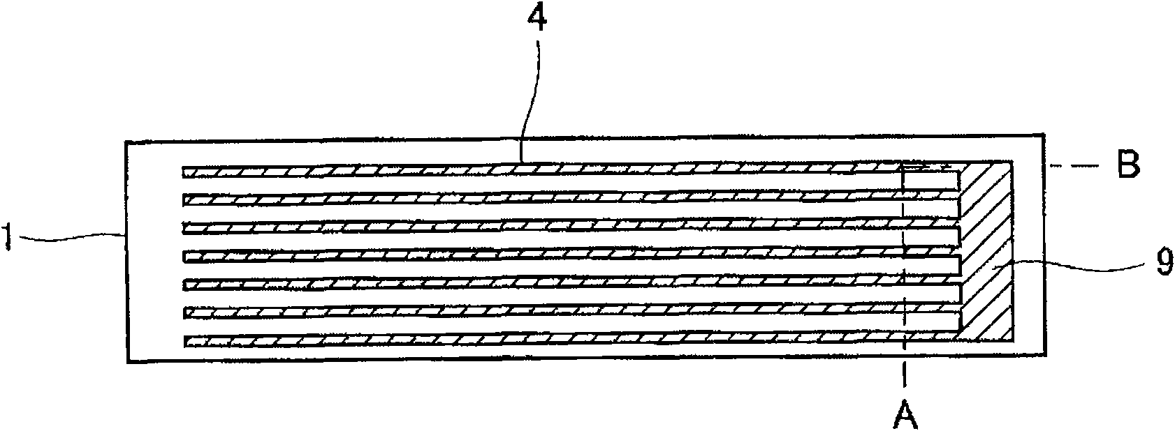
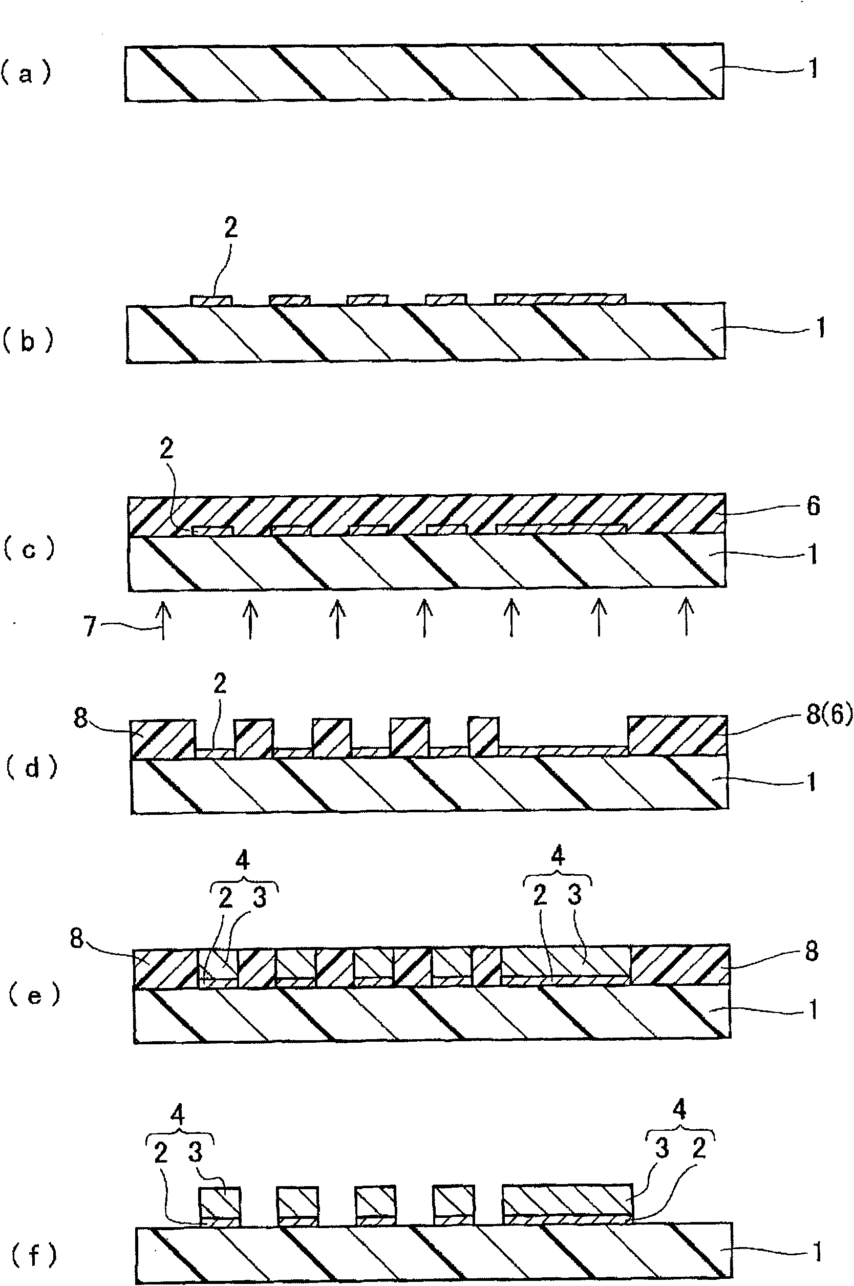
[0065] The printed wiring board of the example of the present invention was produced according to the production method described in the above embodiment.

[0066]The insulating substrate 1 needs to be of a material suitable for exposing the photoresist 6 from the back surface thereof. Commonly used photoresists are often programmed to use UV light exposure. Therefore, considering this as a premise, in this embodiment, as the insulating substrate 1, an insulating film base material for a carrier tape type printed circuit board suitable for a signal transmission path in the millimeter wave band is used. , A sheet of a liquid crystal polymer with a small Tanδ. In addition, the insulating substrate 1 is not limited to liquid crystal polymers, and for example, PET (polyethylene terephthalate, Poly Ethylene Terephthalate), PEN (polyethylene naphthalate, Poly Ethylene Terephthalate) can also be used. Naphthalate), PE (polyethylene, Poly Ethylene), etc., which have good durability ...


PUM

PropertyMeasurementUnit
thicknessaaaaaaaaaa

Abstract

An object of the present invention is to provide the printed wiring board capable of forming fine conductor patterns easily and with high precision, simplifying the manufacturing method and reducing the manufacturing cost. The manufacturing method includes the steps of: forming a base metal pattern on a surface of an insulating substrate; coating the surface with a negative photoresist, where the metal pattern is formed; forming a plating resist pattern on the insulating substrate in such a way that the insulating substrate is irradiated with light so as to transmit therethrough from a surface of the opposite side to the surface of the insulating substrate, and the negative photoresist of a part, where the base metal pattern is not formed, is irradiated with the transmitted light and is exposed with the base metal patterns as a self-alignment mask, and thereafter is developed; and forming a metal pattern selectively on the base metal pattern by plating the surface of the base metal pattern of a part where the plating resist pattern is not formed. In the method, conductor patterns are formed by laminating base metal patterns and plating metal patterns.

Description

technical field [0001] The present invention relates to a printed circuit board and a manufacturing method thereof, and in particular to a printed circuit board suitable for flexible printed circuit boards or TAB tapes having conductive patterns such as wiring patterns on one side of a liquid crystal polymer resin film substrate, and its method of manufacture. Background technique [0002] Printed circuit boards, which are the main part of wiring circuit members of electronic equipment, can generally be roughly classified into rigid printed circuit boards, in which conductive patterns such as wiring patterns are formed on the surface of a hard insulating substrate such as a glass epoxy substrate, and printed circuit boards. A flexible printed wiring board type in which a conductive pattern is formed on the surface of a flexible insulating film substrate such as a polyimide resin film. [0003] In recent years, flexible wiring boards and tape-carriers, which are one type of ...

Claims


Application Information

Patent Timeline
Patent Type & Authority Applications(China)
IPC IPC(8): H05K3/24H05K3/18
CPCH05K2203/0551H05K3/0082H05K3/246H05K3/108H05K3/243H05K2201/0108Y10T29/49155
Inventor 和岛峰生
Owner HITACHI CABLE
Why Eureka
Try Eureka