Multilayer image sensor pixel structure for reducing crosstalk

An image sensor and pixel technology, applied in semiconductor devices, electric solid devices, radiation control devices, etc., can solve problems such as crosstalk

Active Publication Date: 2012-11-28
OMNIVISION TECH INC
View PDF1 Cites 0 Cited by
  • Summary
  • Abstract
  • Description
  • Claims
  • Application Information

AI Technical Summary

Problems solved by technology

[0006] Crosstalk is a serious problem in image sensors

Method used


Image

  • Multilayer image sensor pixel structure for reducing crosstalk
  • Multilayer image sensor pixel structure for reducing crosstalk
  • Multilayer image sensor pixel structure for reducing crosstalk

Examples


Embodiment Construction

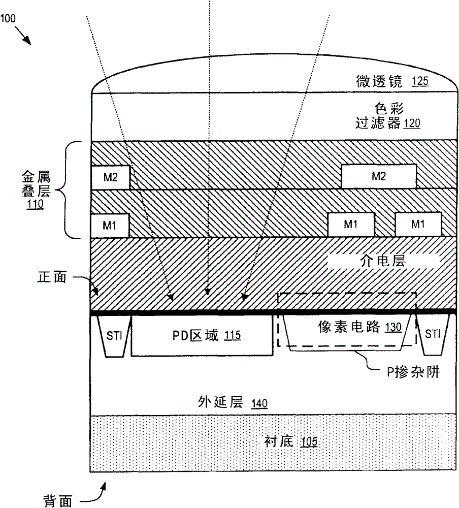
[0021] Embodiments of pixels, image sensors, imaging systems, and methods of fabricating pixels, image sensors, and imaging systems with improved electrical crosstalk characteristics are described herein. In the following description, numerous specific details are set forth in order to provide a thorough understanding of the embodiments. One skilled in the relevant art will recognize, however, that the techniques described herein may be practiced without one or more of these specific details, or with other methods, components, materials, or the like. In other instances, well-known structures, materials, or operations are not shown or described in detail to avoid obscuring certain aspects. For example, although not shown, it should be understood that image sensor pixels (numbered 300, 400, 500, 600, and 700 in the figures) may include multiple layers of material (eg, figure 1 those material layers shown, such as pixel circuitry 130, dielectric layers, metal stack 110, color fi...


PUM


Abstract

An image sensor pixel includes a substrate, a first epitaxial layer, a collector layer, a second epitaxial layer and a light collection region. The substrate is doped to have a first conductivity type. The first epitaxial layer is disposed over the substrate and doped to have the first conductivity type as well. The collector layer is selectively disposed over at least a portion of the first epitaxial layer and doped to have a second conductivity type. The second epitaxial layer is disposed over the collector layer and doped to have the first conductivity type. The light collection region collects photo-generated charge carriers and is disposed within the second epitaxial layer. The light collection region is also doped to have the second conductivity type.

Description

technical field [0001] The present invention relates to a multilayer image sensor pixel structure for reducing crosstalk. Background technique [0002] Image sensors have become ubiquitous. They are widely used in digital still cameras, cellular phones, security cameras, as well as in medical, automotive and other applications. The technology used to fabricate image sensors, particularly complementary metal-oxide-semiconductor ("CMOS") image sensors ("CIS"), has continued to develop at great strides. For example, the need for higher resolution and lower power consumption is driving further miniaturization and integration of these image sensors. [0003] figure 1 The figure shows a conventional front side illuminated CIS pixel 100 . The front side of the CIS pixel 100 is the P+ substrate 105 side on which the pixel circuit 130 is arranged and on which a metal stack 110 for redistributing signals is formed. The metal layers (e.g., metal layers M1 and M2) are patterned in ...

Claims


Application Information

Patent Timeline
Patent Type & Authority Patents(China)
IPC IPC(8): H01L27/146
CPCH01L27/1463H01L27/14601
Inventor 文森特·瓦乃兹艾阿施施·沙哈杨荣生毛杜立钱胤戴幸志霍华德·E·罗兹
Owner OMNIVISION TECH INC
Why Eureka
Try Eureka