
Manufacture method of CMOS (Complementary Metal Oxide Semiconductor) image sensor

A technology of image sensor and manufacturing method, which is applied in semiconductor/solid-state device manufacturing, semiconductor devices, radiation control devices, etc., can solve the problems of high cost, limited area of ​​photodiode active area, etc., and achieve the effect of improving image quality

Active Publication Date: 2012-03-07
SEMICON MFG INT (SHANGHAI) CORP
View PDF0 Cites 0 Cited by
  • Summary
  • Abstract
  • Description
  • Claims
  • Application Information

AI Technical Summary

Problems solved by technology

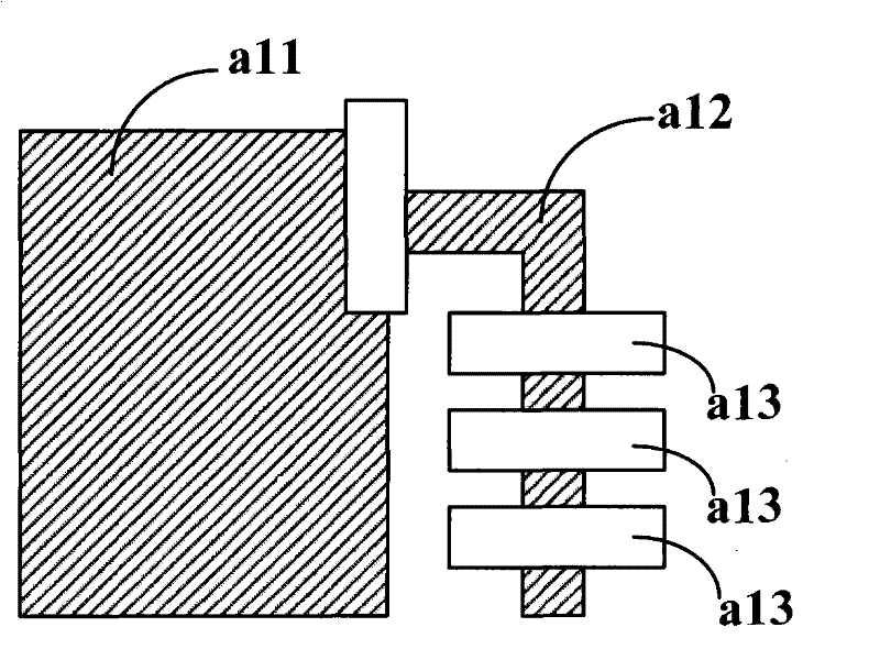
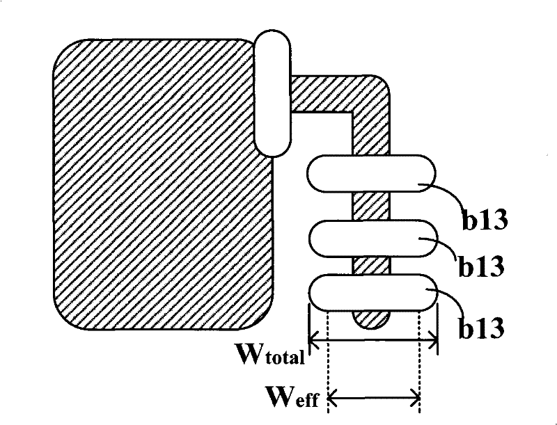
resulting in an effective gate region width W eff less than the actual gate width W total , and the advanced optical proximity calibration correction requires multiple feedback experiments and is expensive, so it is generally only applied to the 90nm and below line width process.
Therefore, in the layout design of the pixel unit, considering the limitations of the semiconductor process, in order to prevent the fabricated pixel unit from failing, the width of the gate region will be appropriately relaxed to meet the effective gate region width W eff practical requirements, which actually limits the area of ​​the active region of the photodiode

Method used


Image

  • Manufacture method of CMOS (Complementary Metal Oxide Semiconductor) image sensor
  • Manufacture method of CMOS (Complementary Metal Oxide Semiconductor) image sensor
  • Manufacture method of CMOS (Complementary Metal Oxide Semiconductor) image sensor

Examples


Embodiment Construction

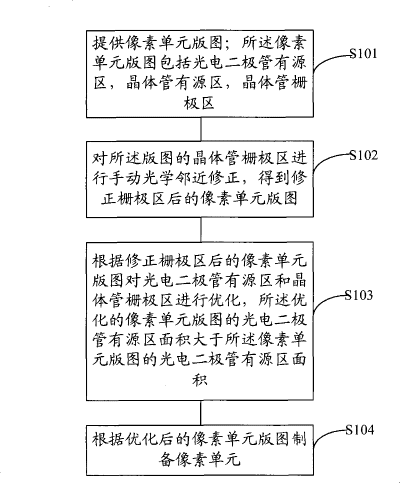
[0013] The present invention provides an embodiment of a manufacturing method of a CMOS image sensor such as image 3 shown, including the following steps:

[0014] Step S101, providing a pixel unit layout; the pixel unit layout includes a photodiode active area, a transistor active area, and a transistor gate area;

[0015] Step S102, performing manual optical proximity correction on the transistor gate area of ​​the layout to obtain the pixel unit layout after the gate area is corrected;

[0016] Step S103, optimize the photodiode active area and transistor gate area according to the pixel unit layout after the gate area is corrected, the photodiode active area area of ​​the optimized pixel unit layout is larger than the photodiode of the pixel unit layout Active area area;

[0017] Step S104, preparing pixel units according to the optimized pixel unit layout.

[0018] In the above implementation manner, by adopting manual optical proximity correction for the gate region ...


PUM


Abstract

The invention relates to a manufacture method of a CMOS (Complementary Metal Oxide Semiconductor) image sensor. The method comprises the following steps of: providing a pixel unit territory comprising a photodiode active region, a transistor active region and a transistor gate region; carrying out manual optical proximity correction on the transistor gate region of the territory to obtain a pixelunit territory subjected to the correction of the gate region; optimizing the original territory according to the pixel unit territory subjected to the correction of the gate region, wherein the areaof the photodiode active region of the optimized pixel unit territory is larger than that of the photodiode active region of the pixel unit territory; and preparing a pixel unit according to the optimized pixel unit territory. The prepared CMOS image sensor meets the requirement for technological parameters of devices, has high fill factor and effectively improves the image quality of the CMOS image sensor.

Description

technical field [0001] The invention relates to the field of semiconductor manufacturing, in particular to a method for manufacturing a CMOS image sensor. Background technique [0002] At present, the charge coupled device (CCD) is the main practical solid-state image sensing device, which has the advantages of low read noise, large dynamic range, and high response sensitivity. The disadvantage of Complementary-Metal-Oxide-Semiconductor (CMOS) technology compatibility is that it is difficult to achieve single-chip integration for image sensors based on charge-coupled devices. The CMOS image sensor (CMOS ImageSensor, CIS) can integrate the pixel array and peripheral circuits on the same chip because of the same CMOS technology. Compared with the charge-coupled device, the CMOS image sensor has small size, light weight, low power Low cost, convenient programming, easy control and low average cost. [0003] A CMOS image sensor includes an array of pixel units, and each pixel ...

Claims


Application Information

Patent Timeline
Patent Type & Authority Patents(China)
IPC IPC(8): H01L21/8238H01L21/027H01L27/146H01L29/06H01L29/423
Inventor 罗飞邹立
Owner SEMICON MFG INT (SHANGHAI) CORP
Learn More