Display device defect detecting method and display device defect detecting device

A technology for display device and defect detection, which is applied in the testing, measuring device, and identification device of machine/structural components, etc., and can solve problems such as non-judgment

Active Publication Date: 2010-10-13
NIKON CORP
View PDF2 Cites 7 Cited by
  • Summary
  • Abstract
  • Description
  • Claims
  • Application Information

AI Technical Summary

Problems solved by technology

[0010] Patent Document 2 selects the resolution of the image according to the type of display defect on the finished product of the liquid crystal display element that becomes the final product, but only for the purpose of finding the defect, and does not judge whether it is a defect that must be repaired

Method used


Image

  • Display device defect detecting method and display device defect detecting device
  • Display device defect detecting method and display device defect detecting device
  • Display device defect detecting method and display device defect detecting device

Examples


Embodiment Construction

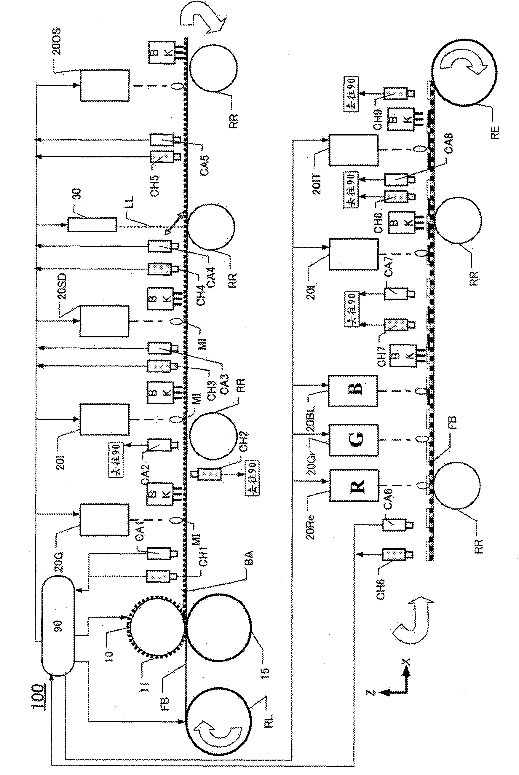
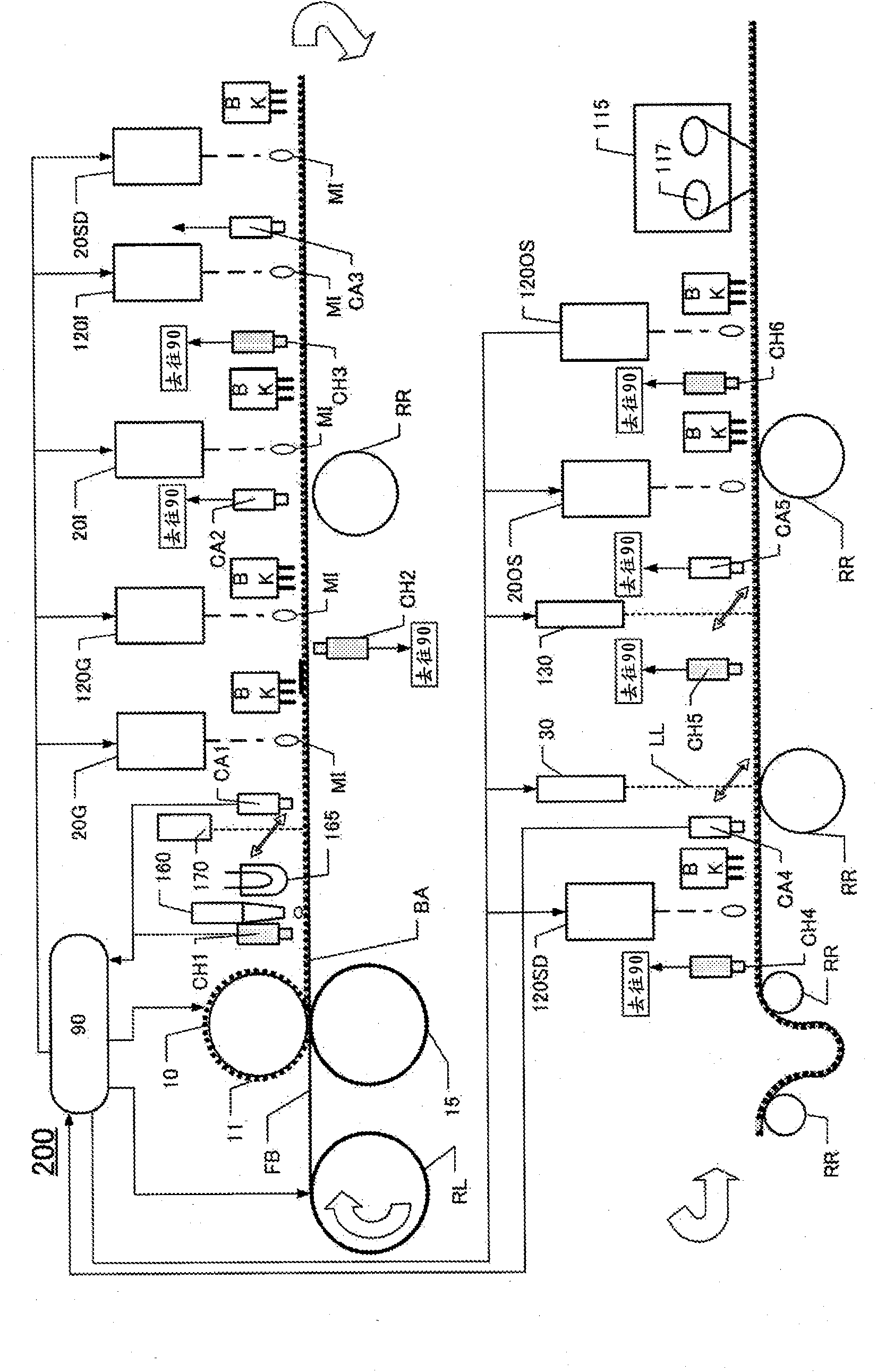
[0038] The manufacturing apparatus of the display element demonstrated in this embodiment mode is an apparatus applicable to an organic EL element, a liquid crystal display element, or a field emission display. The manufacturing apparatus and manufacturing method of an organic EL element are demonstrated as a representative example.

[0039] "Manufacturing device of organic EL element"

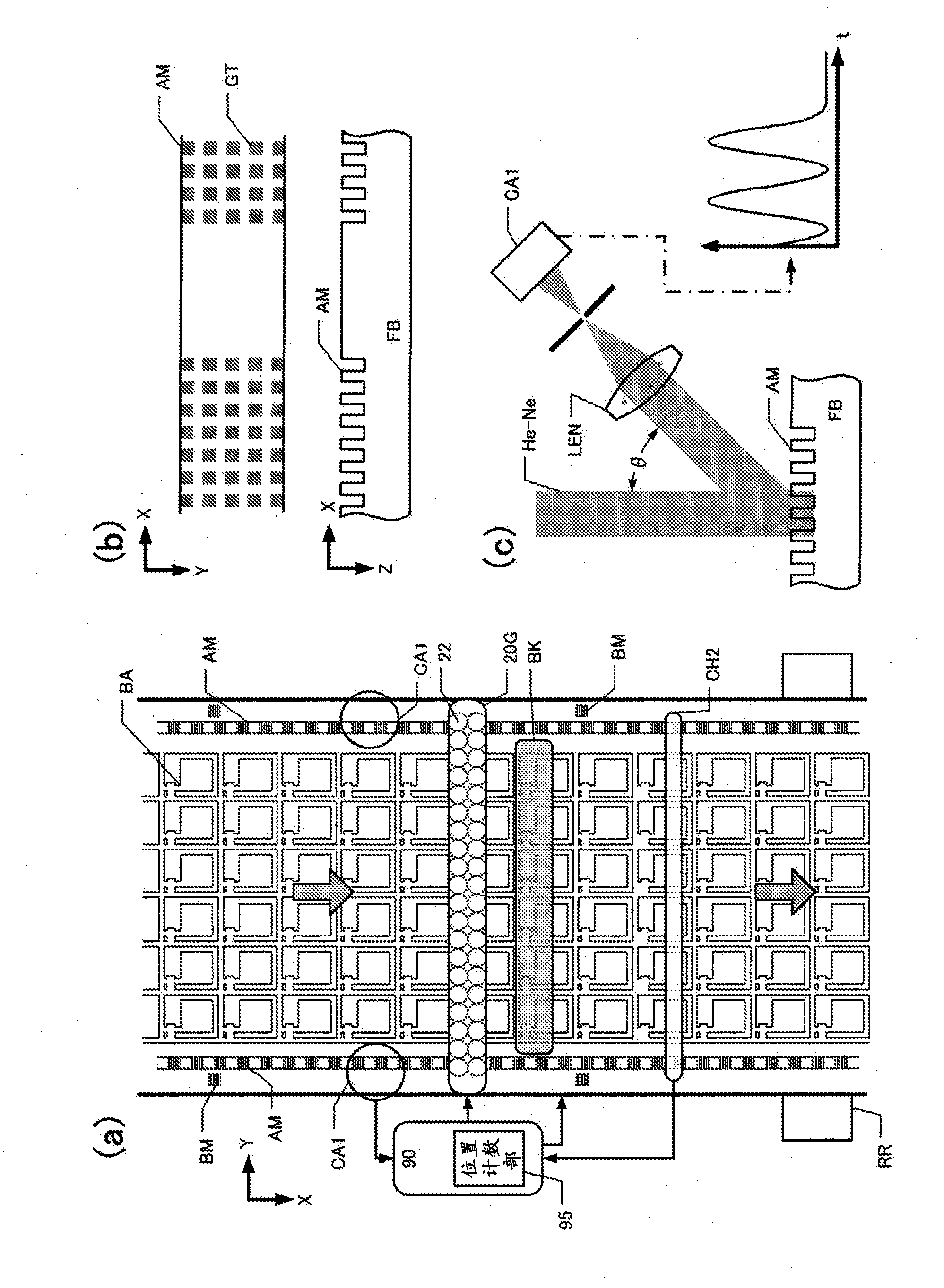
[0040] In the manufacture of an organic EL element, it is necessary to prepare a substrate on which thin film transistors (TFTs) and pixel electrodes are formed. In order to precisely form one or more organic compound layers (light-emitting element layers) including a light-emitting layer on the pixel electrodes on the substrate, it is necessary to form the barrier ribs BA (bank layers) easily and precisely in the boundary region of the pixel electrodes. .

[0041] figure 1 It is a schematic diagram showing the configuration of a manufacturing apparatus 100 for manufacturing an organic EL e...


PUM


Abstract

The invention provides a method for detecting a defect of a display device (50) for judging whether the defect can be repaired in a repair line or the defect requires the manufacturing line to be stopped. A display device defect detecting method comprises a step of measuring a feature value of each partial region of a display device (P32), a defect counting step of counting regions judged to be defective on the basis of the measured feature values (P36), steps of stopping the manufacturing line of the display device if the number of detects counted is larger than a first threshold (P38, P42),a defect density calculating step of calculating the defect density in a predetermined area if the number of defects counted is smaller than the first threshold (P38), and steps of stopping the manufacturing line if the calculated defect density is higher than a second threshold (P40, P42).

Description

technical field [0001] The present invention relates to flat display elements such as organic electroluminescent (EL) elements, liquid crystal display elements, or field emission displays (FED: field emission display). In addition, it relates to a defect detection method and a defect detection device of the display device. Background technique [0002] Display elements such as liquid crystal display elements are widely used in various electronic devices because of their small size, thin shape, low power consumption, and light weight. Driver circuits or thin film transistors that drive these display elements are manufactured using an exposure device generally called a stepper. [0003] However, especially with the advancement of the size of liquid crystal display elements, when the eighth generation or later is reached, due to manufacturing costs, device transportation restrictions, etc., it has reached a point where the existing technology of scaling up and extending the li...

Claims


Application Information

Patent Timeline
IPC IPC(8): G01N21/956G01B11/02G01M11/00G02F1/13G09F9/00H01L51/50H05B33/12
CPCG02F1/136259G01N21/95607G01N2021/9513G01N2021/95615
Inventor 奈良圭浜田智秀
Owner NIKON CORP
Why Eureka
Try Eureka