
Pixel structure of active matrix display device

A technology of display device and pixel structure, which is applied to static indicators, instruments, electrical components, etc., can solve the problems of light leakage, reduce the display contrast value and the life of the light-emitting component 12, and achieve the effect of improving the contrast ratio.

Inactive Publication Date: 2010-10-13
AU OPTRONICS CORP
View PDF0 Cites 22 Cited by
  • Summary
  • Abstract
  • Description
  • Claims
  • Application Information

AI Technical Summary

Problems solved by technology

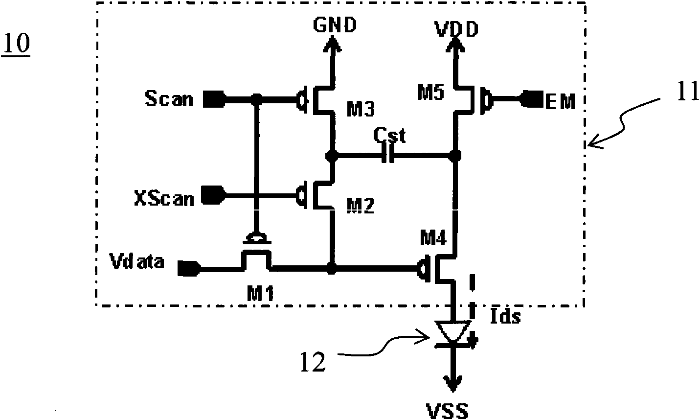
This constant current Ids will cause light leakage, reducing the display contrast value and the life of the light-emitting component 12

Method used


Image

  • Pixel structure of active matrix display device
  • Pixel structure of active matrix display device
  • Pixel structure of active matrix display device

Examples


Embodiment Construction

[0011] In order to have a further understanding of the purpose, structure, features, and functions of the present invention, the following detailed descriptions are provided in conjunction with the embodiments.

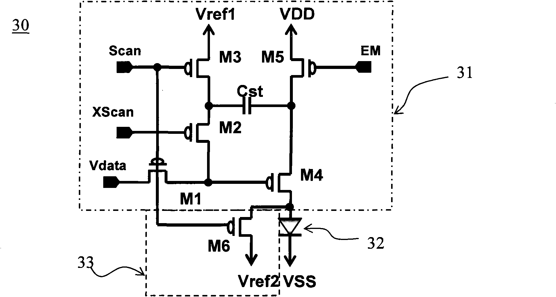
[0012] See image 3 , image 3 It is a circuit diagram of the pixel 30 of the active matrix display device of the present invention. The pixel 30 includes a driving circuit 31 , a light emitting element (OLED) 32 and a shunt circuit 33 . The drive circuit 31 includes a first thin film transistor M1, a second thin film transistor M2, a third thin film transistor M3, a fourth thin film transistor M4, a fifth thin film transistor M5 and a capacitor Cst, wherein the fourth thin film transistor M4 is used to generate a voltage for driving the OLED32. A current is driven to make the OLED 32 emit light. The drain of the first thin film transistor M1 is coupled to the data voltage (Vdata), the gate is coupled to the first scan voltage (Scan), and the source is coupled to t...


PUM


Abstract

The invention discloses a pixel structure of an active matrix display device. The pixel structure comprises a driving circuit, a luminous assembly and a shunt circuit. The driving circuit comprises a first thin film transistor, a second thin film transistor, a third thin film transistor, a fourth thin film transistor, a fifth thin film transistor and a memory capacitor. The positive pole of the luminous assembly is coupled to the drain electrode of the fourth thin film transistor, while the negative pole is coupled to a common voltage. The shunt circuit comprises a sixth thin film transistor, the grid electrode of the six thin film transistor is coupled to a first scanning voltage, the source electrode of the six thin film transistor is coupled to the drain electrode of the fourth thin film transistor, and the drain electrode of the six thin film transistor is coupled to a second reference voltage. The pixel structure can improve the contrast of a displayed picture, and does not reduce the service life of the luminous assembly OLED.

Description

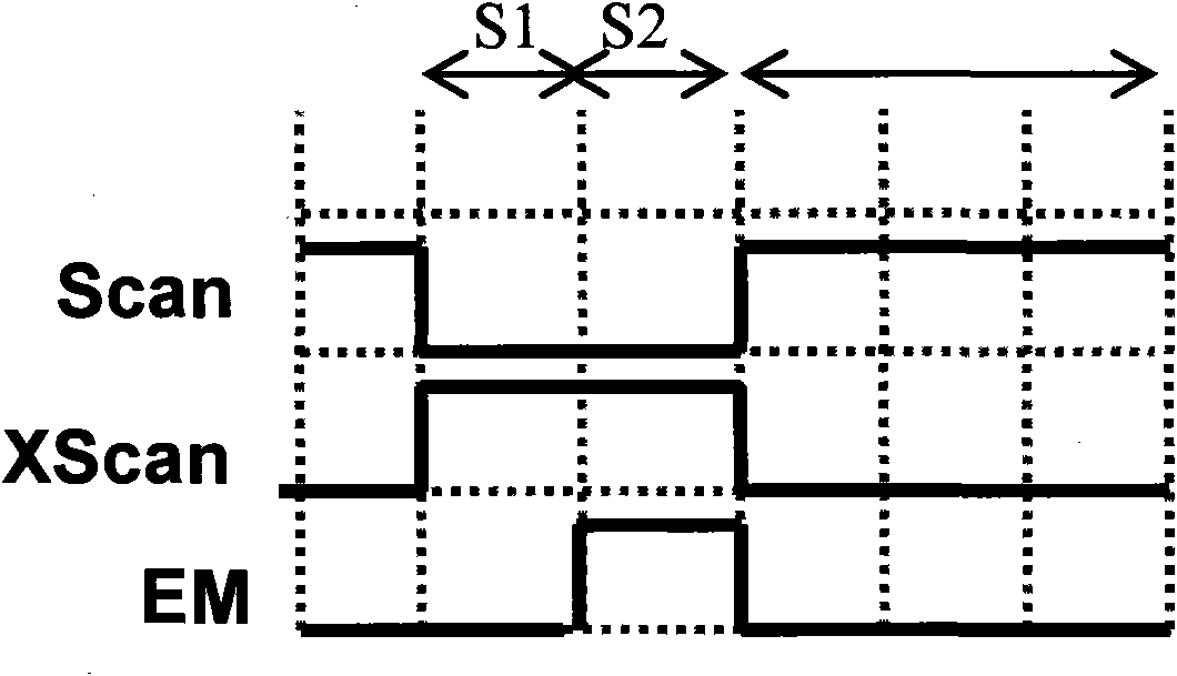
technical field [0001] The present invention relates to a pixel structure of an active matrix display device, in particular to a pixel structure of an active matrix display device with a shunt circuit. Background technique [0002] Currently, organic light emitting diodes (OLEDs) have become the focus of development of new flat panel display panels. OLEDs can be widely used in liquid crystal displays, various backlight sources, communication and digital products, and the like. [0003] See figure 1 , figure 1 It is a circuit diagram of a pixel 10 of a conventional active matrix display device. The pixel 10 includes a well-known driving circuit 11 and a light emitting element (OLED) 12 . The driving circuit 11 includes a first thin film transistor M1, a second thin film transistor M2, a third thin film transistor M3, a fourth thin film transistor M4, a fifth thin film transistor M5 and a capacitor Cst, wherein the fourth thin film transistor M4 is used to generate A curre...

Claims


Application Information

Patent Timeline
Patent Type & Authority Applications(China)
IPC IPC(8): H01L27/32G09G3/32G09G3/20G09G3/325
Inventor 刘俊彦柯凯元蔡轩名吴元均张立勋
Owner AU OPTRONICS CORP
Learn More