Liquid crystal display panel and manufacture method thereof

A technology for liquid crystal display panels and manufacturing methods, which is applied in semiconductor/solid-state device manufacturing, optics, instruments, etc., and can solve problems that affect the display effect of LCD products, reduce production efficiency, and increase production costs, so as to reduce labor costs and maintenance time , Improve yield rate and reduce production cost

Inactive Publication Date: 2010-09-22
BEIJING BOE OPTOELECTRONCIS TECH CO LTD
View PDF0 Cites 10 Cited by
  • Summary
  • Abstract
  • Description
  • Claims
  • Application Information

AI Technical Summary

Problems solved by technology

Although the above two methods can repair the broken data scanning line, it will increase the production cost, and the time spent on maintenance will also reduce the production efficiency. Even after the repair, there will be at least one dead pixel, which will directly affect the display effect of LCD products.

Method used


Image

  • Liquid crystal display panel and manufacture method thereof
  • Liquid crystal display panel and manufacture method thereof
  • Liquid crystal display panel and manufacture method thereof

Examples


Embodiment Construction

[0034] The technical solutions of the present invention will be described in further detail below with reference to the accompanying drawings and embodiments.

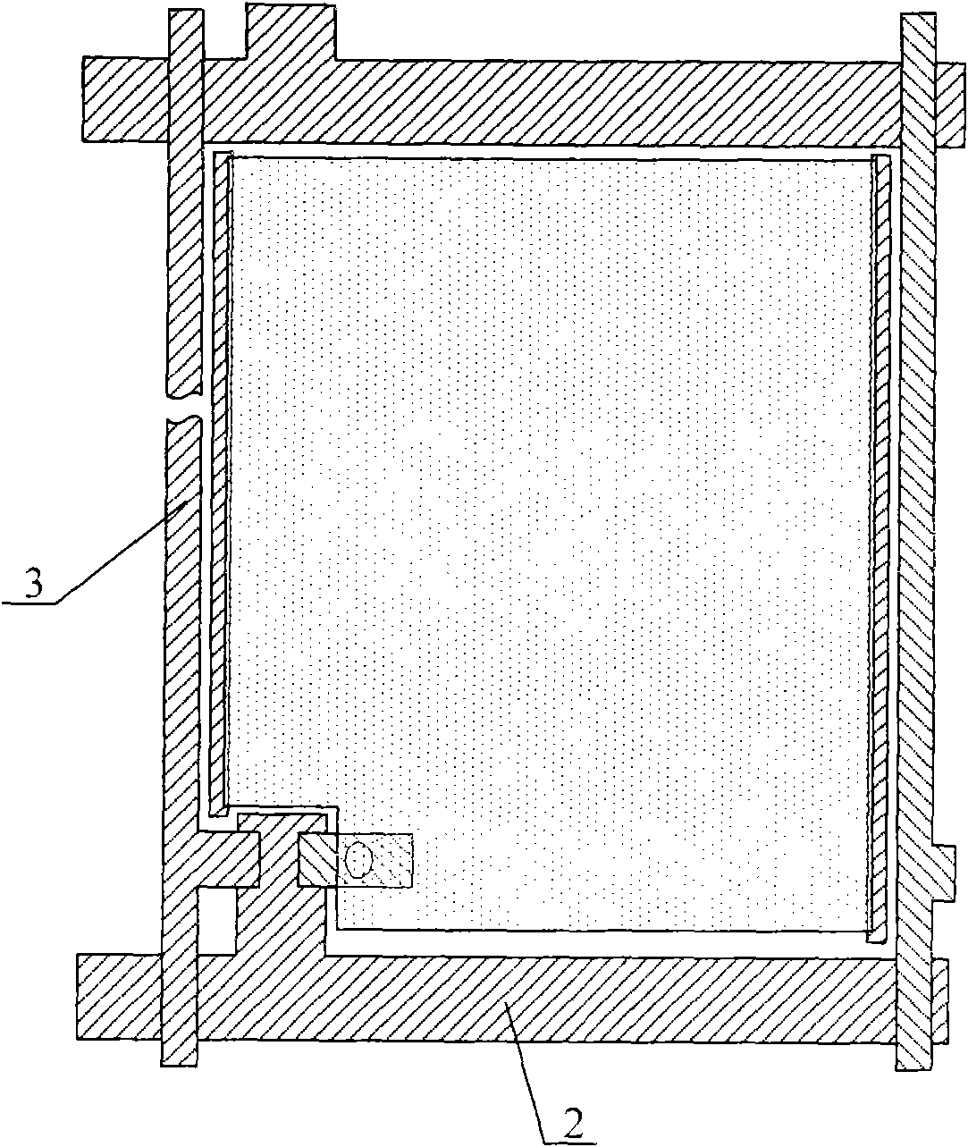
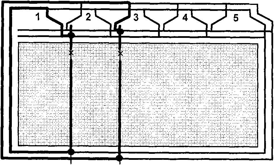
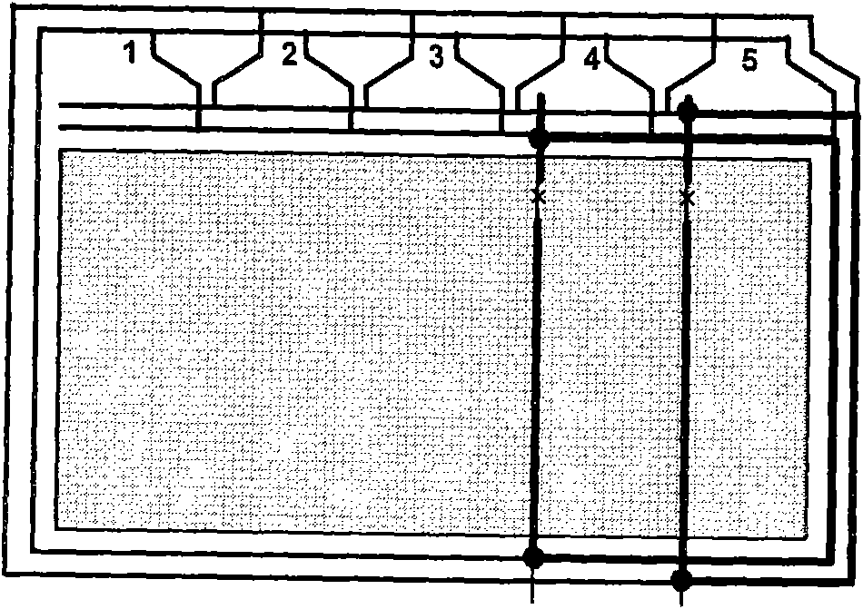
[0035] Figure 6 It is a schematic diagram of the pixel structure of the liquid crystal display panel of the present invention, Figure 7 for Figure 6 Schematic diagram of the cross-section in the direction of A1-A1, Figure 8 for Figure 6 Schematic cross-sectional view of B1-B1 direction. Such as Figure 6 ~ Figure 8 As shown, the liquid crystal display panel provided by this embodiment includes gate lines 2 and data scanning lines 3 formed on the substrate 1, and pixel electrodes and thin film transistors are formed in the pixel area defined by the gate lines 2 and data scanning lines 3, and are perpendicular to each other. The gate line 2 and the data scanning line 3 define the pixel area, the thin film transistor and the pixel electrode are formed in the pixel area, the gate line 2 is used to provide the tur...


PUM


Abstract

The invention relates to a liquid crystal display panel and a manufacture method thereof. The manufacture method of the liquid crystal display panel comprises the following steps: 1. depositing a grid metal film on a substrate, and forming a figure comprising a grid line and a grid electrode by a composition process; 2. depositing a grid insulation film on the substrate completing the step 1 to form a grid insulation layer; 3. depositing a source/drain electrode metal film on the substrate completing the step 2, and forming a figure comprising a source electrode, a drain electrode and a data scanning line by the composition process; 4. depositing a data insulation layer on the substrate completing the step 3, and forming a figure comprising via holes by the composition process; and 5. depositing a nano indium tin metal oxide metal film on the substrate completing the step 4, and forming a figure comprising a data recovery line by the composition process. The invention also provides the liquid crystal display panel. The invention reduces the labor cost and the maintenance time spent for repairing the data scanning line, greatly reduces the production cost and improves the product yield.

Description

technical field [0001] The invention relates to liquid crystal display technology, in particular to a liquid crystal display panel and a manufacturing method thereof. Background technique [0002] Thin Film Transistor Liquid Crystal Display (hereinafter referred to as TFT-LCD) is based on its advantages of excellent performance, good mass production characteristics, and high degree of automation. The application fields are constantly expanding, and more and more LCD products are emerging in electronic products. in the market. The quality of various LCD products has also been greatly tested. Among the many factors affecting the LCD display effect, the data scanning line in the liquid crystal display panel is one of the factors affecting the picture quality. [0003] The manufacturing process of the liquid crystal display panel in the prior art can be summarized as follows: firstly, a gate layer is formed on the substrate, secondly, a gate insulating layer and a semiconductor...

Claims


Application Information

Patent Timeline
Patent Type & Authority Applications(China)
IPC IPC(8): G02F1/1362G02F1/1368H01L21/84H01L27/12
CPCH01L27/124
Inventor 李于华柳奉烈朴相镇
Owner BEIJING BOE OPTOELECTRONCIS TECH CO LTD
Why Eureka
Try Eureka