Side-view type LED packaging structure as well as production method and application thereof

A technology of light-emitting diodes and packaging structures, applied in the directions of optics, light guides, light sources, etc., can solve the problems of uneven thickness, large size, and large difference in expansion coefficient of semiconductor materials of conductive pins 106, and achieve reduced manufacturing difficulty and good heat dissipation Characteristics, Effects of Excellent Thermal Conductivity

Inactive Publication Date: 2012-09-05
CHI MEI LIGHTING TECHNOLOGY CORP
View PDF0 Cites 0 Cited by
  • Summary
  • Abstract
  • Description
  • Claims
  • Application Information

AI Technical Summary

Problems solved by technology

First of all, since the light emitting diode packaging structure 100 is a top view type (Top View Type) light emitting diode structure with a large size, it cannot be applied in a backlight module with a light and thin light guide plate design.
Secondly, the material of the packaging base 102 and the semiconductor material of the LED chip 104 have a large difference in expansion coefficient, which is likely to affect the bonding between the packaging base 102 and the LED chip 104 due to thermal expansion, thereby resulting in the reliability of the LED packaging structure 100. degree drop
Furthermore, the surface of the package base 102 usually needs to be cleaned by plasma during manufacture, but after plasma cleaning, the surface of the package base 102 made of poly-phthalamide is damaged, so that the package base The reflection effect of the surface of 102 becomes worse, which affects the light output
In addition, the design of the heat conduction block 114 makes the thickness of the conductive pins 106 uneven and has a large drop, which will cause the process of making the conductive pins 106 to be too complicated, and will cause residual material problems, which is not conducive to cost reduction.

Method used


Image

  • Side-view type LED packaging structure as well as production method and application thereof
  • Side-view type LED packaging structure as well as production method and application thereof
  • Side-view type LED packaging structure as well as production method and application thereof

Examples


Embodiment Construction

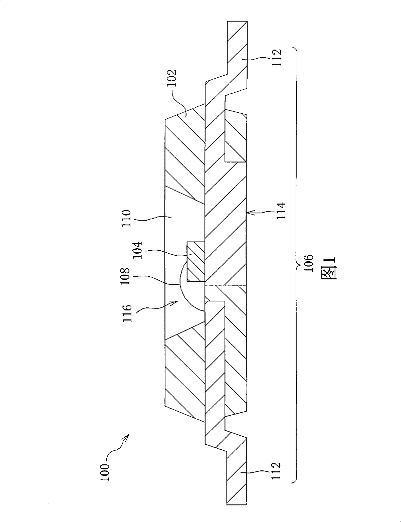
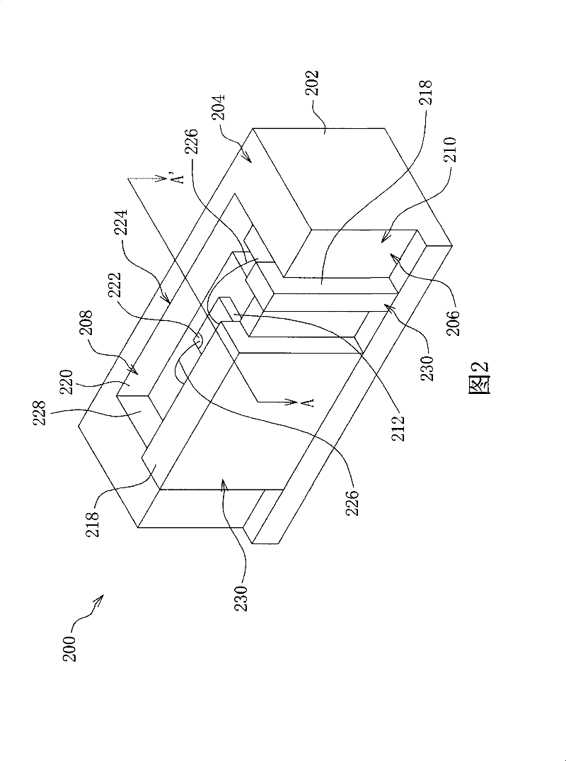
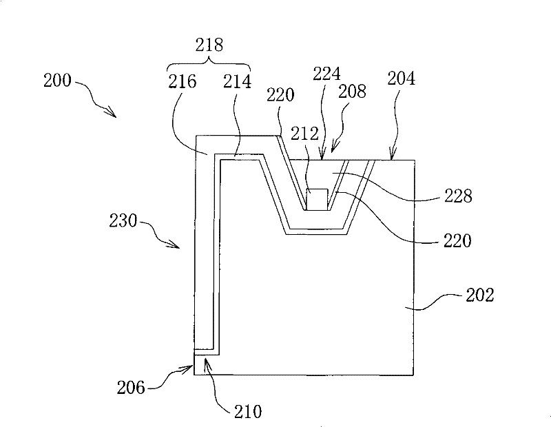
[0060] Please refer to figure 2 and image 3 , which respectively depict a perspective view of a side-view light-emitting diode packaging structure according to a preferred embodiment of the present invention, and along the figure 2 The cross-sectional view of the package structure of the side-view light-emitting diode obtained by the section line AA'. The side-view LED packaging structure 200 mainly includes a silicon base 202 , two conductive pins 218 , one or more LED chips 212 and an encapsulant 228 . In this exemplary embodiment, the silicon base 202 is an integrally formed structure. In one embodiment, the silicon base 202 has adjacent surfaces 204 and 206, wherein the silicon base 202 includes at least a groove 208, and the groove 208 is disposed in the surface 204 of the silicon base 202, wherein the groove 208 defines The light emitting surface 224 of the side-view LED packaging structure 200 is emitted. In the exemplary embodiment, the silicon base 202 further ...


PUM


Abstract

The invention relates to a side-view type LED packaging structure as well as a production method and application thereof. The side-view type LED packaging structure comprises a silicon substrate, a first conducting pin, a second conducting pin and a first LED chip. The silicon substrate comprises a groove which defines the exit surface of the side-view type LED packaging structure; the first conducting pin is positioned on at least part of the groove and extends to one outer surface of the silicon substrate; the second conducting pin is positioned on at least part of the groove and extends to the outer surface of the silicon substrate, and the first conducting pin and the second conducting pin are separated electrically; the first LED chip comprises a first electrode and a second electrode which are respectively electrically connected with the first conducting pin and the second conducting pin in the groove; and the outer surface of the silicon substrate is perpendicular to the exit surface.

Description

technical field [0001] The present invention relates to a light-emitting diode (LED) packaging structure, and in particular to a side-view (Side View Type) light-emitting diode packaging structure and its application on LED light bars and LED backlight modules. Background technique [0002] In the trend of energy saving and environmental protection, light emitting diodes have become the most attractive energy-saving light sources to replace existing light sources. Among light-emitting diode light sources, surface-mounted (SMD) light-emitting diodes are widely used. Since the general LED chip cannot convert most of the input electric energy into light energy, and most of it is lost in the form of heat energy, the conversion efficiency of the LED chip is not high. In addition, if the heat generated during the operation of the LED chip cannot be effectively removed, the junction temperature (Junction Temperature) of the LED chip will rise sharply, which will further lead to a ...

Claims


Application Information

Patent Timeline
Patent Type & Authority Patents(China)
IPC IPC(8): H01L33/00F21S8/00F21V8/00F21V19/00F21Y101/02
Inventor 陈锡铭王星贸
Owner CHI MEI LIGHTING TECHNOLOGY CORP
Why Eureka
Try Eureka