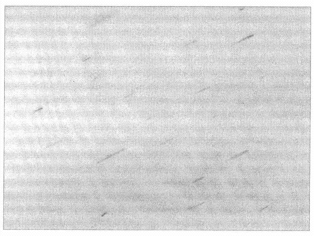
Method for dispersing nanowires based on epoxy resin drawing film
An epoxy resin and nanowire technology, applied in the fields of nanotechnology, nanotechnology, nanostructure manufacturing, etc., can solve problems such as complex processes, and achieve the effect of simple operation process, easy implementation and simple operation.
- Summary
- Abstract
- Description
- Claims
- Application Information
AI Technical Summary
Problems solved by technology
Method used
Image
Examples
Embodiment 1
[0026] Follow the steps below to disperse CdS nanowires on a silicon substrate.
[0027] Step 1: Ultrasonic clean the silicon wafer in alcohol for 10 minutes at room temperature to remove the surface oil, then rinse with distilled water and set aside;
[0028] Step 2: Add 3-4mg of CdS nanowires and 4ml of tetrahydrofuran solution into a test tube with a volume of 15ml, and then perform ultrasonic dispersion treatment at room temperature; then inject 0.7ml of KH560 silicon coupling agent into the tetrahydrofuran solution containing nanowires , stir evenly to obtain a coupling agent treatment solution, in which the nanowires and the inorganic reactive groups of the coupling agent unite to form chemical bonds;
[0029] Step 3: Inject 3.2g of epoxy resin E-44 into the coupling agent treatment solution and stir for 5 minutes to completely dissolve epoxy resin E-44; then inject 2.0g of polyamide resin 650# into it and stir, The polyamide resin 650# was completely dissolved to obtai...
Embodiment 2
[0034] Disperse CdS nanowires on a glass flake substrate as follows.
[0035] Step 1: Ultrasonic clean the glass sheet in alcohol for 10 minutes at room temperature to remove the surface oil, then rinse with distilled water and set aside;
[0036] Step 2: same as step 2 in Example 1;
[0037] Step 3: Inject 3.2g of epoxy resin E-44 into the coupling agent treatment solution and stir for 5 minutes to completely dissolve epoxy resin E-44; then inject 2.0g of 650# polyamide resin into it and stir, Dissolving the polyamide resin to obtain nanowire suspension, the whole process is carried out in a water bath at 35°C; the weight ratio of epoxy resin to polyamide resin is 1.6:1;
[0038] Step 4: Put the nanowire suspensions dissolved with epoxy resin E-44 and polyamide resin 650# respectively in a water bath, set the temperature of the water bath to 35°C, and the water bath time to 21 hours, and ensure that the test tube is well sealed , to prevent the volatilization of tetrahydrof...
Embodiment 3
[0042] Follow the steps below to disperse CdS nanowires on a silicon substrate.
[0043] Step 1: Same as Step 1 in Example 1;
[0044] Step 2: Add 3-4mg of CdS nanowires and 4ml of tetrahydrofuran solution into a test tube with a volume of 15ml, then perform ultrasonic dispersion treatment at room temperature, then add 0.4ml of coupling agent KH560 into the tetrahydrofuran solution containing nanowires, and stir evenly A coupling agent treatment solution is obtained, in which the nanowires and the inorganic reactive groups of the coupling agent unite to form strong chemical bonds;
[0045] Step 3: Inject 2.8g of E-44 epoxy resin into the coupling agent treatment solution, stir for 5 minutes to completely dissolve the epoxy resin, then inject 2.8g of 650# polyamide resin into it and stir to make the polyamide The amide resin is completely dissolved to obtain a suspension of nanowires, and the whole process is carried out in a water bath at 25°C; the weight ratio of epoxy resin...
PUM
 Abstract
Description
Claims
Application Information
 - R&D
- Intellectual Property
- Life Sciences
- Materials
- Tech Scout
- Unparalleled Data Quality
- Higher Quality Content
- 60% Fewer Hallucinations
Browse by: Latest US Patents, China's latest patents, Technical Efficacy Thesaurus, Application Domain, Technology Topic, Popular Technical Reports.
© 2025 PatSnap. All rights reserved.Legal|Privacy policy|Modern Slavery Act Transparency Statement|Sitemap|About US| Contact US: help@patsnap.com


