Display device and method for manufacturing the same

A technology for a display device and a manufacturing method, which is applied in the manufacturing of semiconductor/solid-state devices, organic semiconductor devices, semiconductor devices, etc., can solve problems such as short circuits between lower electrodes and upper electrodes, and achieve the effect of preventing lighting failures

Inactive Publication Date: 2010-06-23
SONY CORP
View PDF2 Cites 4 Cited by
  • Summary
  • Abstract
  • Description
  • Claims
  • Application Information

AI Technical Summary

Problems solved by technology

[0005] In addition, in the organic electroluminescent element having the above-mentioned top emission structure, the electric field is concentrated on a portion where the distance between the lower electrode and the upper electrode is locally narrowed due to the surface roughness of the lower electrode formed of a light-reflective metal material, and as a result, Prone to short circuit between lower and upper electrodes

Method used


Image

  • Display device and method for manufacturing the same
  • Display device and method for manufacturing the same
  • Display device and method for manufacturing the same

Examples


Embodiment Construction

[0020] Hereinafter, embodiments of the present invention will be described in detail in the order of the structure of a display device and its manufacturing method with reference to the accompanying drawings.

[0021] Structure of the display device of the first embodiment

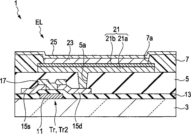
[0022] figure 1 is a cross-sectional view of the structure of one pixel of the display device according to the first embodiment. The display device 1 shown in this figure is an active matrix display device including an organic electroluminescence element EL, and is structured as follows.

[0023] Specifically, a thin film transistor Tr is provided in each pixel on the substrate 3 , and the thin film transistor Tr is covered with the interlayer insulating film 5 . A connection hole 5 a extending to the thin film transistor Tr is provided in the interlayer insulating film 5 . Further, in each pixel on the interlayer insulating film 5, an organic electroluminescence element EL connected to the thin film tr...


PUM

PropertyMeasurementUnit
thicknessaaaaaaaaaa
thicknessaaaaaaaaaa
thicknessaaaaaaaaaa

Abstract

A display device is provided which includes: lower electrodes each have a light-reflective first metal material layer and a second metal material layer provided thereon which has a superior alkaline-solution resistance to that of the first metal material layer; an insulating pattern which is formed from a photosensitive composition material, which has opening portions to expose the lower electrodes, and which covers peripheries of the lower electrodes; organic layers each of which at least include an organic light emitting layer and which are provided in the opening portions so as to cover the lower electrodes; and a light-transmissive upper electrode provided to sandwich the organic layers with the lower electrodes.

Description

technical field [0001] The present invention relates to a display device and a manufacturing method thereof, and more particularly, to a display device including an organic electroluminescent element and a method for manufacturing the display device. Background technique [0002] An organic electroluminescence element utilizing electroluminescence (hereinafter referred to as "EL") of an organic material has an organic hole transport layer and a layer laminated thereon between a lower electrode and an upper electrode serving as an anode or a cathode. An organic layer of an organic light-emitting layer, and has attracted attention as a light-emitting element capable of emitting high-brightness light by low-voltage DC driving. [0003] An active matrix display device using the above-mentioned organic electroluminescent element has a structure in which an organic electroluminescent element is provided on an interlayer insulating film covering a pixel driving circuit formed of a ...

Claims


Application Information

Patent Timeline
Patent Type & Authority Applications(China)
IPC IPC(8): H01L27/32H01L51/52H01L21/82H01L51/56
CPCH01L27/3246H01L27/3274H01L2251/5315H01L51/5218H10K59/125H10K59/122H10K50/818H10K2102/3026H10K50/11H10K71/00
Inventor 平井畅一
Owner SONY CORP
Why Eureka
Try Eureka