Long laminated sub-wave reflection-reducing structure and preparation method thereof
A sub-wavelength, stacked technology, applied in the field of micro-nano photonics, can solve problems such as the overall performance limitation of the device
- Summary
- Abstract
- Description
- Claims
- Application Information
AI Technical Summary
Problems solved by technology
Method used
Image
Examples
Embodiment Construction
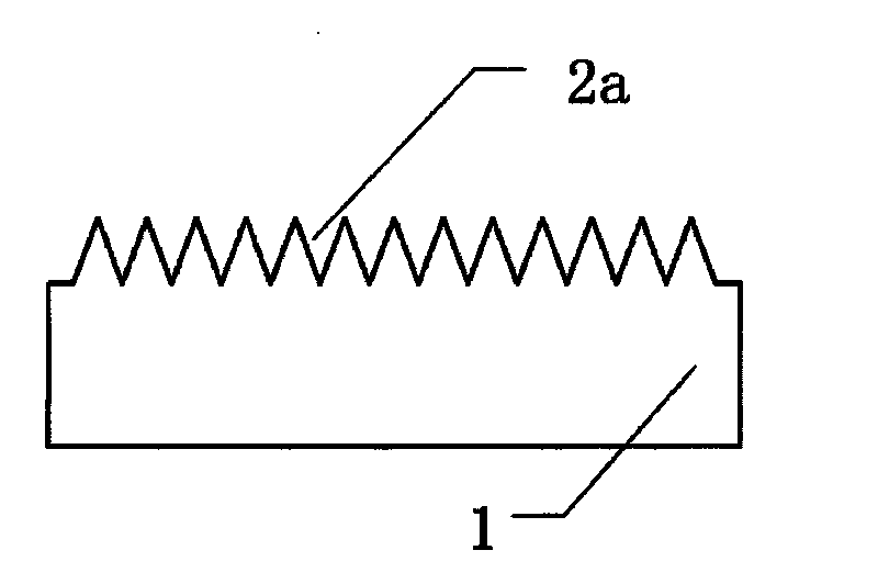
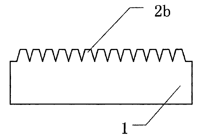
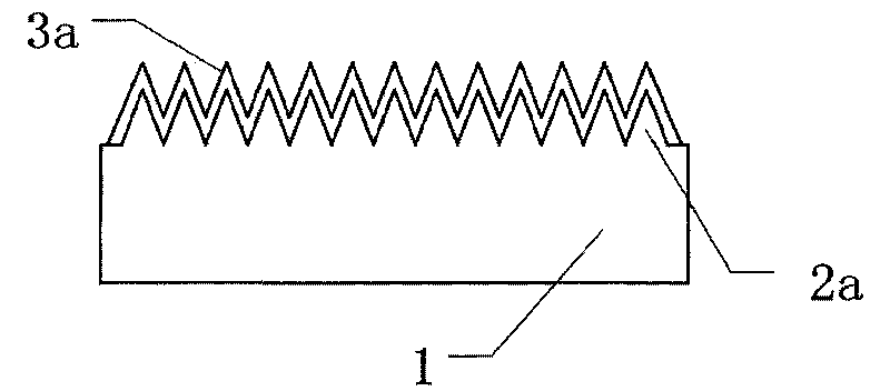
[0028] In order to break through the limitation of the existing sub-wavelength structure in improving the overall performance of the device, the present invention discloses a laminated sub-wavelength anti-reflection structure, and the shape of the sub-wavelength anti-reflection structure is calculated according to the wavelength and angle range of the incident light to be de-reflected. It is characterized in that: the laminated subwavelength antireflection structure includes two parts: the first part is to form a subwavelength pattern on the surface of the high refractive index material that needs antireflection by etching; the second part is to form a subwavelength pattern on the first part of the subwavelength pattern The surface of the dielectric layer is re-deposited and grown, and the two are integrated to form a stacked sub-wavelength anti-reflection structure.
[0029] The subwavelength antireflection structure can be prepared by the following technical solutions:
[00...
PUM
| Property | Measurement | Unit |
|---|---|---|
| refractive index | aaaaa | aaaaa |
Abstract
Description
Claims
Application Information
 - Generate Ideas
- Intellectual Property
- Life Sciences
- Materials
- Tech Scout
- Unparalleled Data Quality
- Higher Quality Content
- 60% Fewer Hallucinations
Browse by: Latest US Patents, China's latest patents, Technical Efficacy Thesaurus, Application Domain, Technology Topic, Popular Technical Reports.
© 2025 PatSnap. All rights reserved.Legal|Privacy policy|Modern Slavery Act Transparency Statement|Sitemap|About US| Contact US: help@patsnap.com


