
Method for detecting positional deviation among layers of multilayer printed circuit board

A printed circuit board, inner layer technology, applied in the direction of measuring electricity, measuring devices, measuring electrical variables, etc., can solve the problems of high time-consuming and cost, unable to represent the degree of alignment, unfavorable and accurate judgment of the degree of alignment, etc. Improve work efficiency

Inactive Publication Date: 2011-07-13
ELEC & ELTEK GUANGZHOU ELECTRONICS
View PDF0 Cites 2 Cited by
  • Summary
  • Abstract
  • Description
  • Claims
  • Application Information

AI Technical Summary

Problems solved by technology

In actual production, this measurement method requires quality inspection personnel to make slices and judge with the naked eye. However, due to certain differences among different people, the inspection results will be uneven, and even defective products may be misjudged as good products; This test method requires the actual slicing process, and the measurement efficiency is extremely low; at the same time, the method of slicing is bound to damage the circuit board, resulting in unnecessary scrapping
When the number of single-layer boards is large in the concentric circle alignment method, too many concentric circles will not be conducive to the computer's accurate judgment of the alignment, while the longitudinal slicing method is not only time-consuming and costly, but also due to the position of the hole when drilling. , different directions and angles affect the correctness of the computer's judgment of alignment
Furthermore, when applied to a large-area multilayer printed circuit board, in addition to the relative offset between each single-layer board, it also causes inconsistent alignment of each position due to different degrees of thermal expansion and contraction. The alignment obtained by the concentric circle alignment method or the longitudinal slicing method cannot represent the actual alignment of each position of each single-layer board. The quality of the circuit board

Method used

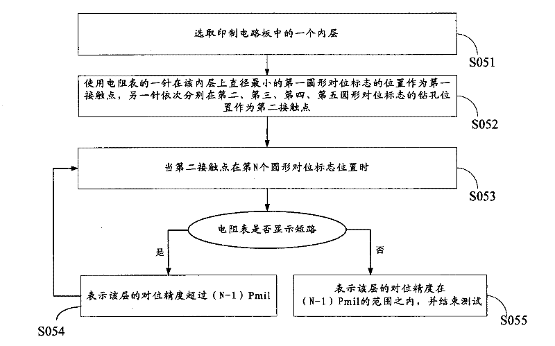
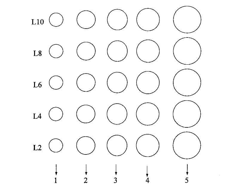

Image

  • Method for detecting positional deviation among layers of multilayer printed circuit board
  • Method for detecting positional deviation among layers of multilayer printed circuit board
  • Method for detecting positional deviation among layers of multilayer printed circuit board

Examples


Embodiment Construction

[0028] In order to make the present invention easier to understand, the present invention will be further described in conjunction with the accompanying drawings, but the embodiments in the accompanying drawings do not constitute any limitation to the present invention.

[0029] The invention relates to a manufacturing method of a multilayer printed circuit board, in particular to a judging method for judging whether the positions between layers are shifted during the manufacturing process of the multilayer printed circuit board. It can meet the interlayer offset judgment requirements of all products.

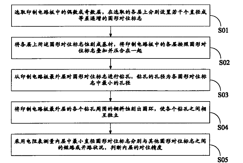
[0030] figure 1 A flow chart of a method for detecting position deviation between layers of a multilayer printed circuit board according to an embodiment of the present invention is shown.

[0031] The method includes the following steps:

[0032] Step S01, select the even-numbered or odd-numbered layers in the printed circuit board, and set a number of circular alignment mar...


PUM


Abstract

The invention discloses a method for detecting positional deviation among layers of a multilayer printed circuit board, which comprises the following steps: A, selecting an even layer or an odd layer in the printed circuit board, and setting a plurality of circular alignment marks of which the diameters are in equidifferent and progressive increase on the selected layers; B, etching the circular alignment marks on the layers to form substrates, and overlying and pressing the layers in the printed circuit board into a whole according to the circular alignment marks; C, drilling holes on the circular alignment marks from the outermost layer of the printed circuit board, wherein the bore diameters of drilling holes are the minimum bore diameter in the circular alignment marks; D, etching copper materials around the drilling holes at the outermost layer of the printed circuit board to form circular rings so as to enable the drilling holes to be independent mutually; and E, measuring the short-circuit or open-circuit situation between the circular alignment mark with the minimum diameter and the other circular alignment marks by adopting an ohmmeter to judge the alignment accuracy of an inner layer. The method can detect the positional deviation among the layers of the multilayer printed circuit board simply and quantitatively.

Description

technical field [0001] The invention relates to a quality detection method of a multilayer printed circuit board, in particular to a method for detecting positional deviation between layers of a multilayer printed circuit board. Background technique [0002] With the development of printed circuit boards towards high density, the structure of multilayer circuit boards is the most commonly used type. Each layer of the multilayer printed circuit board consists of upper and lower inner layers of copper foil and an insulating layer located in between. The materials of each layer are combined with semi-cured glue as an adhesive and bonded by pressing. Wherein, the layers of copper foils are in a non-communicating state. Therefore, in order to connect some or specific parts of the circuits of each layer, it is necessary to form a through hole by drilling, and then go through the step of electroplating the through hole, so that the inner wall surface of the through hole and the ou...

Claims


Application Information

Patent Timeline
Patent Type & Authority Patents(China)
IPC IPC(8): G01R31/02
Inventor 崔赛华
Owner ELEC & ELTEK GUANGZHOU ELECTRONICS
Learn More