
Touch-control sensing structure for liquid crystal display

A liquid crystal display, touch sensing technology, applied in static indicators, instruments, electric solid devices, etc., can solve the problems of decreased light transmittance, inconsistent with the lightness, thinness and shortness of the display, and increased reflectivity.

Inactive Publication Date: 2009-12-30
CHI HSIN ELECTRONICS CORP
View PDF0 Cites 7 Cited by
  • Summary
  • Abstract
  • Description
  • Claims
  • Application Information

AI Technical Summary

Problems solved by technology

[0002] figure 1 Shown is a commonly used liquid crystal display structure with touch function, which includes a display panel 1 and a touch panel 2, the display panel 1 has upper and lower substrates 1a, 1b and a liquid crystal layer 1c, and for the purpose of coloring is more A color filter layer 1d is arranged between the upper substrate 1a and the liquid crystal layer 1c, and for the convenience of manipulation, the touch panel 2 is pasted on the outside of the upper substrate 1a. The control panel 2 is an independent component and is attached to the display panel 1 in a laminated manner. Therefore, the total weight of the display will be increased, and the touch panel 2 must be formed by laminating two transparent substrates 2a, 2b. Therefore, the overall thickness of the display will be increased. The aforementioned situation obviously does not meet the market's expectations for light, thin, and short displays.
[0003] Secondly, because the touch panel 2 is installed on the side close to the viewer, when the displayed image passes through the two transparent substrates 2a, 2b and appears outside, the two transparent substrates 2a, 2b will inevitably affect the image. For example, the light transmittance decreases or the reflectivity increases, which will reduce the optical display effect of the display

Method used


Image

  • Touch-control sensing structure for liquid crystal display
  • Touch-control sensing structure for liquid crystal display
  • Touch-control sensing structure for liquid crystal display

Examples


Embodiment Construction

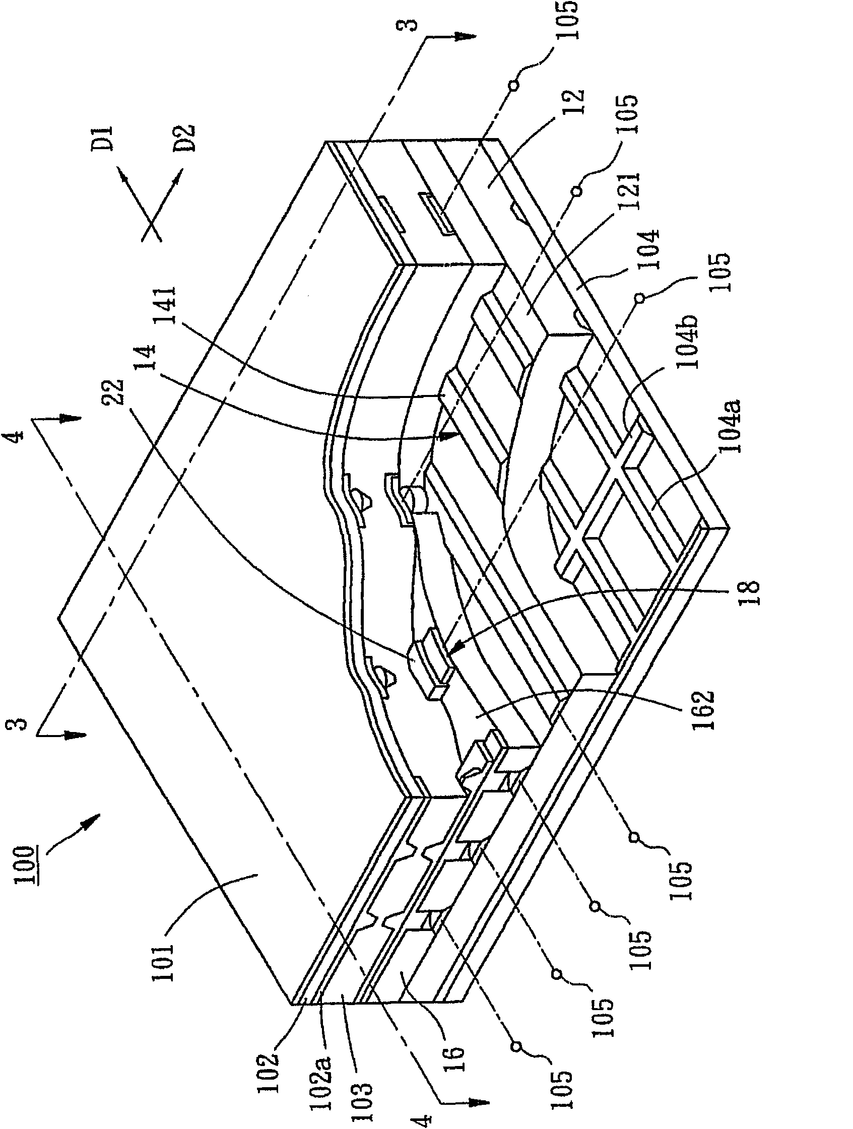
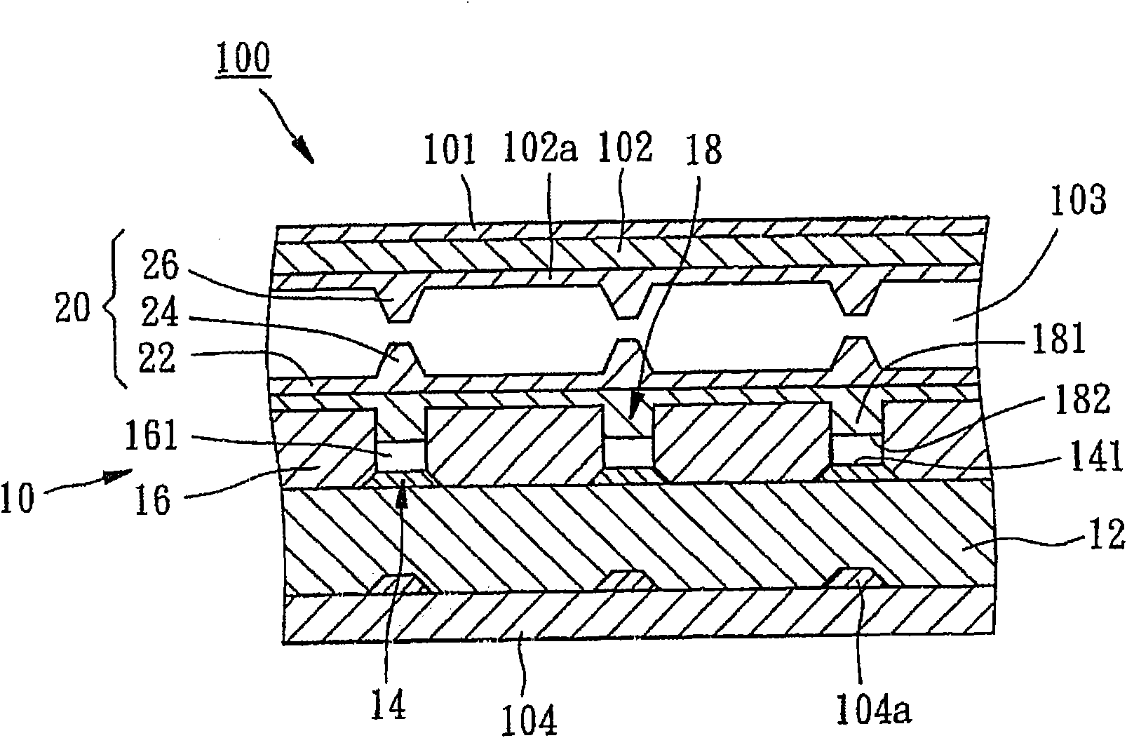
[0039] Figure 2 to Figure 4 Disclosed is a liquid crystal display 100 comprising a touch sensing structure 10 according to a preferred embodiment of the present invention. The structure of the liquid crystal display 100 includes an upper substrate 101, a color filter layer 102, a liquid crystal layer 103 and a bottom substrate from top to bottom. The substrate 104, wherein the color filter layer 102 includes a plurality of red, green and blue filter units (not shown), and a filter unit for isolating these red, green and blue filter units to avoid The black matrix 102a in which the filter units interfere with each other, the lower substrate 104 is a thin film transistor array substrate, including a plurality of data lines 104a and a plurality of scanning lines 104b interlaced with each other. Since the above components belong to the existing structure, here I won't go into details.

[0040] The touch sensing structure 10 of this embodiment includes a first insulating layer 12...


PUM


Abstract

The invention discloses a touch-control sensing structure for a liquid crystal display, which is arranged between a liquid crystal layer and a thin film transistor array substrate of the liquid crystal display. The touch-control sensing structure comprises a plurality of first electrodes, a plurality of second electrodes, and an insulating layer for generating electrical isolation between the first electrodes and the second electrodes, wherein the insulating layer is provided with a punch hole structure at the overlapping junctions of the first electrodes and the second electrodes, the second electrodes completely cover and joint to the periphery of punch holes, and under the action of external force pressing, the second electrodes corresponding to a pressed part contact with the first electrodes through the punch holes so as to generate resistance impedance effect and judge the position of the pressing point.

Description

technical field [0001] The present invention is related to liquid crystal displays, and more specifically refers to a touch sensing structure for liquid crystal displays. Background technique [0002] figure 1 Shown is a commonly used liquid crystal display structure with touch function, which includes a display panel 1 and a touch panel 2, the display panel 1 has upper and lower substrates 1a, 1b and a liquid crystal layer 1c, and for the purpose of coloring is more A color filter layer 1d is arranged between the upper substrate 1a and the liquid crystal layer 1c, and for the convenience of manipulation, the touch panel 2 is pasted on the outside of the upper substrate 1a. The control panel 2 is an independent component and is attached to the display panel 1 in a laminated manner. Therefore, the total weight of the display will be increased, and the touch panel 2 must be formed by laminating two transparent substrates 2a, 2b. Therefore, the overall thickness of the displa...

Claims


Application Information

Patent Timeline
IPC IPC(8): G02F1/133G06F3/041G02F1/1362H01L27/12
Inventor 赖辉龙
Owner CHI HSIN ELECTRONICS CORP
Learn More