Electrostatic discharge protection pattern for high voltage applications
By using separate N+S/D island implant patterning and oxide doped isolation areas in semiconductor devices, the problem of insufficient ESD protection in high-voltage environments is solved, achieving higher current limit and device durability, and avoiding equipment Premature failure and safety risks.
- Summary
- Abstract
- Description
- Claims
- Application Information
AI Technical Summary
Problems solved by technology
Method used
Image

Examples
Embodiment Construction
[0029] The making and utilization of presently preferred embodiments are described in detail below. It should be appreciated, however, that the present invention provides many applicable inventive concepts that can be embodied in a wide variety of specific situations. The specific embodiments discussed are only intended to illustrate the making and use of the present invention in specific ways, and are not intended to limit the scope of the present invention.
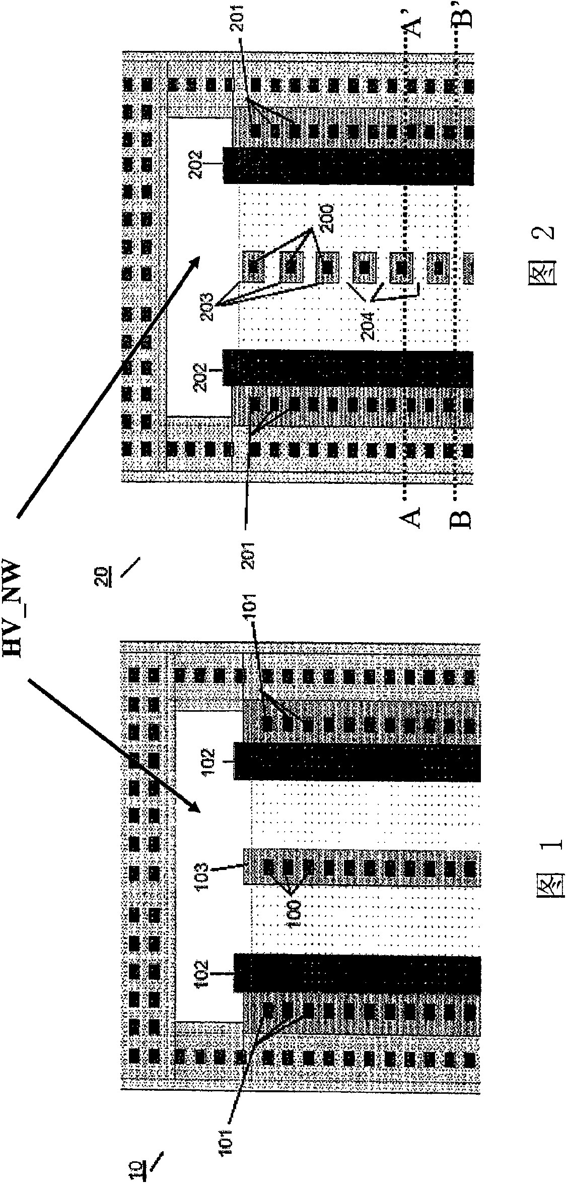
[0030] now refer to figure 1 , shows a gap with zero N + Plan view of transistor group 10 with doped S / D regions 103 . The transistor group 10 includes S / D contact holes 100 and 101 , and a gate 102 . By setting N at the S / D contact hole 100+ The doped region provides ESD protection for the transistor group 10 . Although the zero gap N + Doped region 103 reduces breakdown that occurs at high voltage operation, but lateral and other breakdown current leakage associated with ESD still continues to be experienced in t...
PUM
 Abstract
Description
Claims
Application Information
 - R&D
- Intellectual Property
- Life Sciences
- Materials
- Tech Scout
- Unparalleled Data Quality
- Higher Quality Content
- 60% Fewer Hallucinations
Browse by: Latest US Patents, China's latest patents, Technical Efficacy Thesaurus, Application Domain, Technology Topic, Popular Technical Reports.
© 2025 PatSnap. All rights reserved.Legal|Privacy policy|Modern Slavery Act Transparency Statement|Sitemap|About US| Contact US: help@patsnap.com