Semiconductor laser and manufacturing method therefor
一种制造方法、半导体的技术,应用在半导体激光器、激光器、激光器零部件等方向,能够解决成品率下降、不能正常地生长、半导体激光器特性降低等问题,达到好漏电流的效果
- Summary
- Abstract
- Description
- Claims
- Application Information
AI Technical Summary
Problems solved by technology
Method used
Image


Examples
Embodiment approach 1
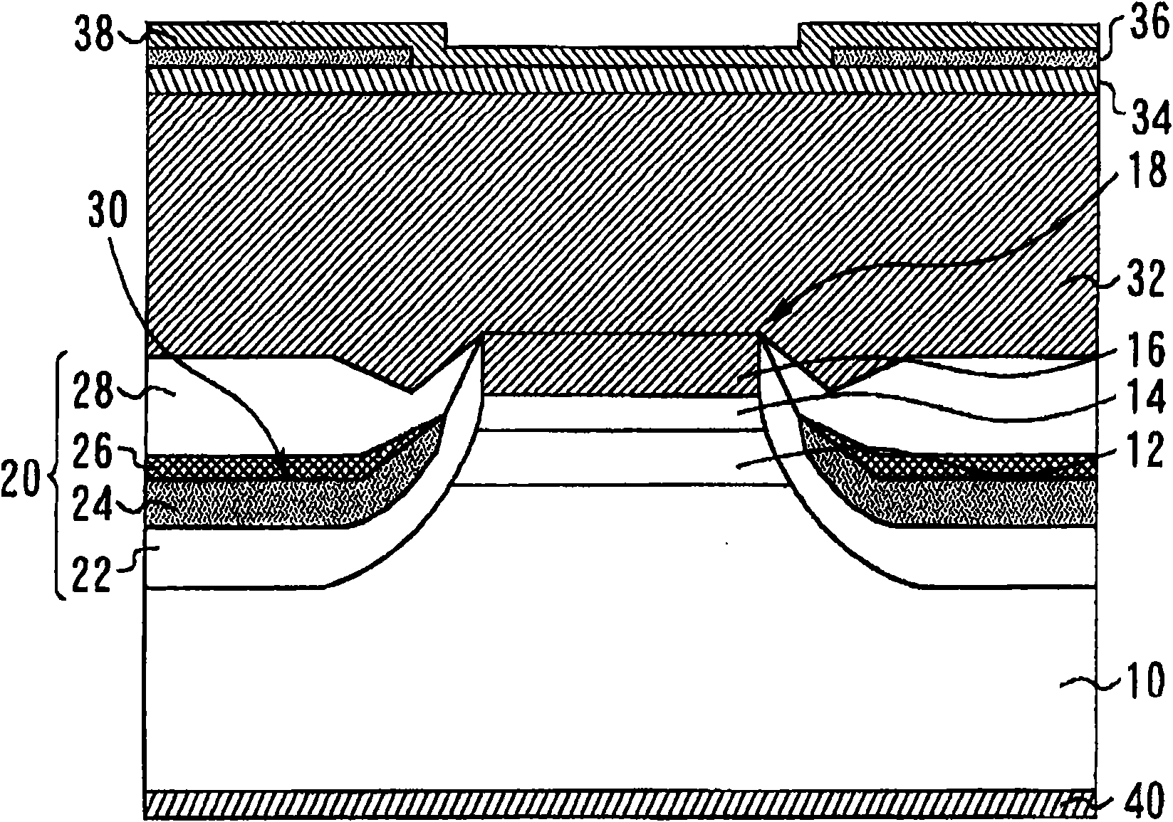
[0029] figure 1 is a cross-sectional view showing the semiconductor laser according to Embodiment 1 of the present invention. A ridge structure 18 is formed on a p-type InP substrate 10 (semiconductor substrate), and the ridge structure 18 is a p-type InP cladding layer 12 (p-type cladding layer), an AlGaInAs strained quantum well (strained quantumwell) active layer 14 ( active layer) and n-type InP cladding layer 16 (n-type cladding layer). Here, the carrier concentration of the p-type InP cladding layer 12 is 1×10 18 cm -3 , the carrier concentration of the n-type InP cladding layer 16 is 1×10 18 cm -3 .
[0030] Both sides of the ridge structure 18 are buried with the buried layer 20 . The buried layer 20 has a p-type InP layer 22 , an n-type InP layer 24 , a low-carrier-concentration p-type InP layer 26 , and a p-type InP layer 28 in this order from below. Low carrier concentration p-type InP layer 26 (p-type semiconductor layer) and n-type InP layer 24 (n-type semi...
Embodiment approach 2
[0040] image 3 It is a cross-sectional view showing a semiconductor laser according to Embodiment 2 of the present invention. A low carrier concentration n-type InP layer 44 is provided instead of the low carrier concentration p-type InP layer 26 . The carrier concentration of the low carrier concentration n-type InP layer 44 is 1×10 17 cm -3 . The p-type InP layer 28 (p-type semiconductor layer) and the low carrier concentration n-type InP layer 44 (n-type semiconductor layer) constitute a pn junction 46 . Other structures are the same as those in Embodiment 1.
[0041] In the semiconductor laser of this embodiment mode, the low carrier concentration n-type InP layer 44 is inserted, and the n-type carrier concentration of the pn junction 46 is changed from the conventional 1×10 19 cm -3 Reduced to 1×10 17 cm -3 . Therefore, the capacitance C of the pn junction 46 can be reduced to 0.9 pF, and the cutoff frequency fc is 22 GHz, so high-speed modulation of 10 Gbps or ...
Embodiment approach 3
[0043] Figure 4 It is a cross-sectional view showing a semiconductor laser according to Embodiment 3 of the present invention. The conductivity type of the substrate is different from that of the first embodiment.
[0044] On n-type InP substrate 50 (semiconductor substrate), form ridge structure 18, and this ridge structure 18 is to n-type InP cladding layer 52 (n-type cladding layer), AlGaInAs strained quantum well active layer 54 (active layer) and The p-type InP cladding layer 56 (p-type cladding layer) is laminated. Here, the carrier concentration of the n-type InP cladding layer 52 is 1×10 18 cm -3 , the carrier concentration of the p-type InP cladding layer 56 is 1×10 18 cm -3 .
[0045] Both sides of the ridge structure 18 are buried with the buried layer 20 . The buried layer 20 has a p-type InP layer 58 , a low carrier concentration p-type InP layer 60 , an n-type InP layer 62 , and a p-type InP layer 64 in order from below. Low carrier concentration p-type ...
PUM
 Abstract
Description
Claims
Application Information
 - R&D
- Intellectual Property
- Life Sciences
- Materials
- Tech Scout
- Unparalleled Data Quality
- Higher Quality Content
- 60% Fewer Hallucinations
Browse by: Latest US Patents, China's latest patents, Technical Efficacy Thesaurus, Application Domain, Technology Topic, Popular Technical Reports.
© 2025 PatSnap. All rights reserved.Legal|Privacy policy|Modern Slavery Act Transparency Statement|Sitemap|About US| Contact US: help@patsnap.com