Liquid crystal display device

A technology of a liquid crystal display device and a liquid crystal layer, which is applied to instruments, semiconductor devices, optics, etc., can solve the problem that the third liquid crystal display device 3 cannot achieve electrical neutrality, etc., and achieves the effect of solving image sticking and avoiding inaccurate compensation.

Active Publication Date: 2009-11-25
SHANGHAI TIANMA MICRO ELECTRONICS CO LTD
View PDF0 Cites 5 Cited by
  • Summary
  • Abstract
  • Description
  • Claims
  • Application Information

AI Technical Summary

Problems solved by technology

However, this compensation method will also bring new problems: since the third common electrode 332 is kept consistent in the third lower substrate 310, only the mode of horizontal frequency inversion of the potential of the third common electrode 332 can be adopted. The potential of the row third pixel electrode 331 is overall compensated
[0009] Please refer to Figure 4(a) and Figure 4(b) in conjunction with figure 1 , as the working time of the third liquid crystal display device 3 in FFS mode increases, some of the charges generated by polarization are pinned on the dielectric layer due to the existence of the DC component of the current between the third upper substrate 300 and the third lower substrate 310 The surface, specifically, is mainly pinned on the alignment film (not shown) of the third upper substrate 300, so that the inside of the third liquid crystal display device 3 in FFS mode cannot achieve electrical neutrality.

Method used


Image

  • Liquid crystal display device
  • Liquid crystal display device
  • Liquid crystal display device

Examples


no. 1 example

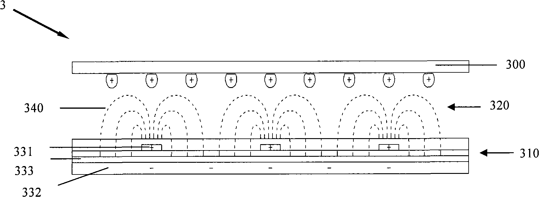
[0052] See Figure 5 , And refer to Figure 6 The first liquid crystal display device 1 in FFS (Fringe field switch) mode includes an upper substrate 100, a lower substrate 110 facing the upper substrate 100, and a lower substrate 110 sandwiched between the upper substrate 100 and the lower substrate 110. The liquid crystal layer 120. A number of data lines 111 and gate lines 112 perpendicular to each other are arranged on the lower substrate 110 of the first liquid crystal display device 1. The data line 111 and the gate line 112 define a number of pixel regions 113.

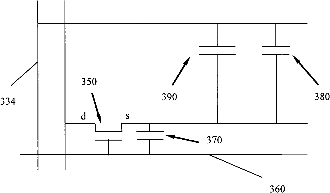
[0053] See Figure 7 , And refer to Figure 5 versus Picture 9 ,among them, Picture 9 It is a schematic diagram of an equivalent circuit of the first liquid crystal display device 1 in the FFS mode. A comb-shaped first pixel electrode 114 is formed in each pixel area 113 of the lower substrate 110. The comb-shaped first pixel electrode 114 is electrically connected to the first thin film transistor 130. The capac...

no. 2 example

[0059] Refer below Picture 9 , Picture 10 and Picture 11 The second embodiment of the present invention will be described. The second embodiment is different from the first embodiment in that the liquid crystal display device of the second embodiment is an IPS mode liquid crystal display device. The same parts as in the first embodiment use the same reference numerals, and will not be repeated here.

[0060] See Picture 10 , And refer to Picture 11 The second liquid crystal display device 2 in IPS (In Plane Switching) mode includes an upper substrate 100, a lower substrate 110 facing the upper substrate 100, and a lower substrate 110 sandwiched between the upper substrate 100 and the lower substrate 110. The liquid crystal layer 120. A number of data lines 111 and gate lines 112 perpendicular to each other are arranged on the lower substrate 110 of the liquid crystal display device 2. The data line 111 and the gate line 112 define a number of pixel regions 113.

[0061] Please ...


PUM


Abstract

The invention discloses a liquid crystal display device which comprises an upper baseplate and a lower baseplate, wherein the lower baseplate is arranged facing to the upper baseplate; the lower baseplate is provided with a plurality of gate lines, data lines and common lines; the gate lines and the data lines are mutually vertical and definite a plurality of pixel areas. Each pixel area comprises pixel electrodes, common electrodes, a first thin film transistor, a second thin film transistor and a liquid crystal layer, wherein the common electrodes and the pixel electrodes are arranged in a staggered way; the first thin film transistor is used for controlling the pixel electrodes and inputting signals; the second thin film transistor is used for controlling the common electrodes and inputting signals; the liquid crystal layer is sandwiched between the upper baseplate and the lower baseplate; and when the first thin film transistor is switched off, the second thin film transistor is also switched off at the same time. Feed-through potential drop of an entire row of the gate lines does not need to be adjusted by potential provided by the common lines through the structural design, thereby the phenomenon of residual DC can not be produced, and the problem of residual shade can be fundamentally solved.

Description

Technical field [0001] The present invention relates to a liquid crystal display device, in particular to a liquid crystal display device capable of reducing feed-through potential drop. Background technique [0002] IPS (In-plane switch) liquid crystal display mode is a wide viewing angle liquid crystal display mode. Because of its excellent viewing angle characteristics, it has been widely used in liquid crystal display products, especially in large-size liquid crystal display products. IPS technology is a liquid crystal display mode with different optical path differences caused by the in-plane flip of liquid crystal molecules according to the lateral electric field, so as to realize the liquid crystal display mode with different light transmittance. The original design of the IPS liquid crystal display mode was to arrange the strip-shaped common electrode and the pixel electrode on the same plane. [0003] The FFS (Fringe field switch) mode liquid crystal display device is fo...

Claims


Application Information

Patent Timeline
IPC IPC(8): G02F1/1362H01L27/12
Inventor 马骏蒋顺凌志华
Owner SHANGHAI TIANMA MICRO ELECTRONICS CO LTD
Why Eureka
Try Eureka