Thin film transistor

A thin film transistor and carbon nanotube thin film technology, applied in the field of thin film transistors based on carbon nanotubes, can solve the problems of poor transmission performance, poor flexibility of thin film transistors, unfavorable thin film transistors, etc., and achieve excellent mechanical properties, good toughness and mechanical strength. , the effect of improving the response speed

Inactive Publication Date: 2009-11-18
TSINGHUA UNIV +1
View PDF0 Cites 3 Cited by
  • Summary
  • Abstract
  • Description
  • Claims
  • Application Information

AI Technical Summary

Problems solved by technology

Since carbon nanotubes have good carrier axial transport properties, but poor radial transport properties, carbon nanotubes arranged perpendicular to the substrate direction are also unfavorable for obtaining thin films with high carrier mobility. transistor
Therefore, the above two arrangements of carbon nanotubes cannot effectively utilize the high carrier mobility of carbon nanotubes.
Therefore, thin film transistors using disordered carbon nanotube layers or carbon nanotube arrays as semiconductor layers in the prior art are not conducive to obtaining thin film transistors with higher carrier mobility and higher response speed, and in the prior art The thin film transistors are less flexible

Method used


Image

  • Thin film transistor
  • Thin film transistor
  • Thin film transistor

Examples


Embodiment Construction

[0012] The thin film transistor provided by the embodiment of the technical solution will be described in detail below with reference to the accompanying drawings.

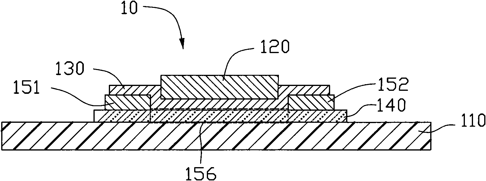
[0013] see figure 1 , the first embodiment of the technical solution provides a thin film transistor 10, the thin film transistor 10 is a top gate type, which includes a semiconductor layer 140, a source 151, a drain 152, an insulating layer 130 and a gate 120 . The TFT 10 is formed on a surface of an insulating substrate 110 .

[0014] The semiconductor layer 140 is disposed on the surface of the insulating substrate 110 . The source 151 and the drain 152 are spaced apart on the surface of the semiconductor layer 140 . The insulating layer 130 is disposed on the surface of the semiconductor layer 140 . The gate 120 is disposed on the surface of the insulating layer 130 and is insulated from the semiconductor layer 140 and the source 151 and the drain 152 through the insulating layer 130 . A region of the sem...


PUM


Abstract

The invention relates to a thin film transistor, comprising a source electrode, a leakage electrode, a semiconductor layer and a grid electrode. The leakage electrode and the source electrode at intervals; the grid electrode, the semiconductor layer, the source electrode and the leakage electrode are arranged in an insulating way through an insulating layer, wherein the semiconductor layer comprises a plurality of carbon nano tubes, and two ends of at least part of the carbon nano tubes are electrically connected with the source electrode and the leakage electrode respectively.

Description

technical field [0001] The invention relates to a thin film transistor, in particular to a thin film transistor based on carbon nanotubes. Background technique [0002] Thin Film Transistor (TFT) is a key electronic component in modern microelectronics technology, and has been widely used in fields such as flat panel displays. A thin film transistor mainly includes a gate, an insulating layer, a semiconductor layer, a source and a drain. Wherein, the source and the drain are arranged at intervals and electrically connected with the semiconductor layer, and the gate is insulated from the semiconductor layer and the source and the drain through the insulating layer. A region of the semiconductor layer between the source and the drain forms a channel region. The gate, source, and drain in the thin film transistor are all made of conductive materials, and the conductive materials are generally metals or alloys. When a voltage is applied to the gate, the channel region in the ...

Claims


Application Information

Patent Timeline
Patent Type & Authority Applications(China)
IPC IPC(8): H01L29/786H01L29/06
CPCB82Y10/00H01L51/0541H01L51/0048H01L51/0545H01L51/0558H01L51/0012H10K71/191H10K85/221H10K10/466H10K10/464H10K10/484
Inventor 姜开利李群庆范守善
Owner TSINGHUA UNIV
Why Eureka
Try Eureka