A semiconductor material property measurement device and method based on double probe beam
A technology of material characteristics and measuring devices, which is applied in the direction of color/spectral characteristic measurement, measuring devices, material analysis through optical means, etc., can solve problems such as difficulty in the same position, increase equipment cost, etc., to improve reliability and Accuracy, the effect of improving measurement accuracy
Inactive Publication Date: 2011-01-05
INST OF OPTICS & ELECTRONICS - CHINESE ACAD OF SCI
View PDF2 Cites 0 Cited by
- Summary
- Abstract
- Description
- Claims
- Application Information
AI Technical Summary
Problems solved by technology
Sometimes it is necessary to use these two independent measurement methods to measure the characteristic parameters of semiconductor materials at the same time in the application. If the measurement is carried out by two sets of independent measurement devices, it is difficult to ensure that the measurement is carried out at the same position, and the equipment will be increased. cost
Method used
View moreImage
Smart ImageViewing Examples

Examples
Embodiment Construction
Login to View More PUM
| Property | Measurement | Unit |
|---|---|---|
| electrical resistivity | aaaaa | aaaaa |
| electrical resistivity | aaaaa | aaaaa |
| reflectance | aaaaa | aaaaa |
Abstract
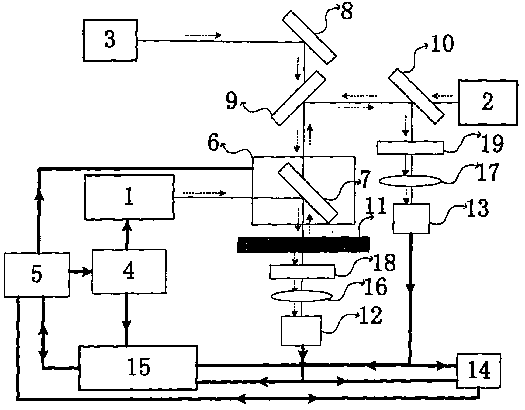
The invention is a semiconductor material property measurement device and method based on double probe beam for measuring the characteristic parameters of semiconductor materials and monitoring the doping process. It obtains the free carrier absorption signal and the light-modulated reflecting signal simultaneously in the same set of test system based on the absorption of the exciting light of theperiodic intensity modulation by the semiconductor materials; it obtains the free carrier absorption signal and light-modulated reflecting signal of the frequency domain by changing the modulation frequency of the exciting light; it obtains the free carrier absorption signal and light-modulated reflecting signal of the spatial domain by changing the spacing between the exciting light and the probe light; it may obtain the characteristic parameters of semiconductor materials and the process parameters as the doping concentration through the analysis and processing of the signals obtained or the comparison with the signal data of the calibration sample. The invention makes up for the shortcomings of the single technology and improves the measurement accuracy; it obtains two kinds of signalssimultaneously in one device and more important parameters of the semiconductor materials comparing with the single technology.
Description
Device and method for measuring characteristics of semiconductor materials based on dual probe beams technical field The invention belongs to the technical field of non-destructive testing of semiconductor materials, and in particular relates to a measuring device and a measuring method for determining semiconductor material characteristics by combining free carrier absorption technology and light modulation reflection technology, that is, double detection beam detection technology. Background technique Only by doping the semiconductor material to change its structure and resistivity, the semiconductor material can become a useful functional material. The precise monitoring of the impurity concentration doped in the semiconductor material and the processing technology such as annealing determines the performance of the semiconductor device to a large extent. In the monitoring process, some characteristic parameters of semiconductor materials are measured to judge whether t...
Claims
Login to View More Application Information
Patent Timeline
 Patent Type & Authority Patents(China)
IPC IPC(8): G01N21/31G01N21/17G01N21/88G01R27/02
Inventor 李斌成黄秋萍刘显明韩艳玲
Owner INST OF OPTICS & ELECTRONICS - CHINESE ACAD OF SCI
Features
- R&D
- Intellectual Property
- Life Sciences
- Materials
- Tech Scout
- Unparalleled Data Quality
- Higher Quality Content
- 60% Fewer Hallucinations
Learn More Browse by: Latest US Patents, China's latest patents, Technical Efficacy Thesaurus, Application Domain, Technology Topic, Popular Technical Reports.
© 2025 PatSnap. All rights reserved.Legal|Privacy policy|Modern Slavery Act Transparency Statement|Sitemap|About US| Contact US: help@patsnap.com