Electronic component mounting board, method for manufacturing the same and electronic circuit unit
A technology for installing electronic components and conductive components, which is applied in the direction of assembling printed circuits, circuits, and contact components with electric components, which can solve problems such as increased inductance and difficult application of high-frequency electronic components, and achieves the reduction of electrode intervals and shortened conduction. through part, the effect of reducing inductance
- Summary
- Abstract
- Description
- Claims
- Application Information
AI Technical Summary
Problems solved by technology
Method used
Image

Examples
no. 1 approach
[0068] Hereinafter, the present invention will be described in detail with reference to the drawings, but the present invention is not limited thereto, and various changes can be made without departing from the gist of the present invention.
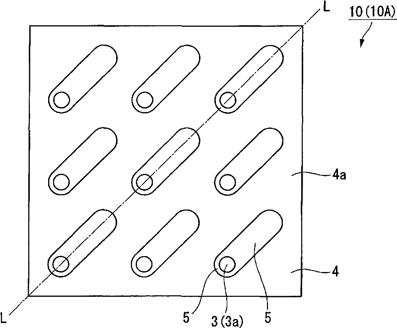
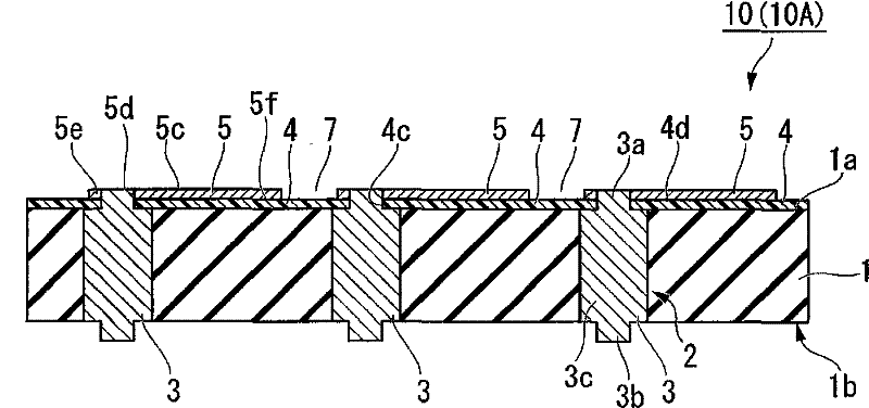
[0069] Figure 1A , 1B It is a figure which schematically shows 1st Embodiment of the board|substrate 10 (10A) for mounting electronic components of this invention. Figure 1A is a top view, Figure 1B yes Figure 1A The L-L section diagram.
[0070] The electronic component mounting substrate 10A of the present invention is roughly composed of the following components: a base 1, which is made of a flat elastic body, and has a plurality of through holes 2 arranged in parallel at predetermined intervals; a conductive member 3, which It is arranged so that the main body portion 3c is filled in the through hole 2, and has a first protruding portion 3a and a second protruding portion 3b at one end and the other end respectively, the firs...
no. 2 approach
[0097] Figure 7A , 7B It is a figure which schematically shows the board|substrate 10 (10B) for electronic component mountings concerning 2nd Embodiment of this invention. The same symbols are assigned to the same parts as those in the first embodiment, and their descriptions are omitted. Figure 7A is a top view, Figure 7B yes Figure 7A The L-L section diagram. This embodiment differs from the first embodiment in that a slit 9 is arranged on the substrate 4 along the shape of the other end 5 f of the electrode 5 .
[0098] The slit 9 has only to be arranged so as to surround at least the outer periphery of the electrode 5 on the side of the one end 5 f. The slit 9 increases the stroke amount of the electrode 5, and when the electronic component 60 is mounted in the same manner as the first embodiment, it is possible to further absorb the variation in the height of the solder bump α. Therefore, the contact pressure of the electrode 5 with the solder bump α of the elec...
no. 3 approach
[0101] Figure 8A , 8B It is a figure which schematically shows the board|substrate 10 (10C) for electronic component mountings concerning 3rd Embodiment of this invention. The same symbols are assigned to the same parts as in the second embodiment, and their descriptions are omitted. Figure 8A is a top view, Figure 8B yes Figure 8A The L-L section diagram. This embodiment differs from the second embodiment in that structures 6 ( 6 a , 6 b ) are arranged on both surfaces 1 a , 1 b of a base 1 .
[0102] By providing substrates 4 (4a, 4b) with electrodes 5 (5a, 5b) arranged on both surfaces 1a, 1b of the base body 1, that is, structures 6 (6a, 6b) as in this embodiment, it is possible to mount electronic components. At the same time, height deviations are more effectively absorbed on both sides of the base body 1 . Therefore, the electronic components 60 or the circuit board 70 having different heights can be mounted on both sides, and the electronic circuit components...
PUM
 Abstract
Description
Claims
Application Information
 - R&D
- Intellectual Property
- Life Sciences
- Materials
- Tech Scout
- Unparalleled Data Quality
- Higher Quality Content
- 60% Fewer Hallucinations
Browse by: Latest US Patents, China's latest patents, Technical Efficacy Thesaurus, Application Domain, Technology Topic, Popular Technical Reports.
© 2025 PatSnap. All rights reserved.Legal|Privacy policy|Modern Slavery Act Transparency Statement|Sitemap|About US| Contact US: help@patsnap.com