Manufacturing method of electrophoresis display device, electrophoresis display device, and electronic apparatus
A technology of electrophoretic display and manufacturing method, which is applied in the direction of semiconductor/solid-state device manufacturing, circuits, electrical components, etc., which can solve the problems of uneven electrical characteristics and achieve the effect of preventing malfunction
- Summary
- Abstract
- Description
- Claims
- Application Information
AI Technical Summary
Problems solved by technology
Method used
Image
Examples
Embodiment approach 2
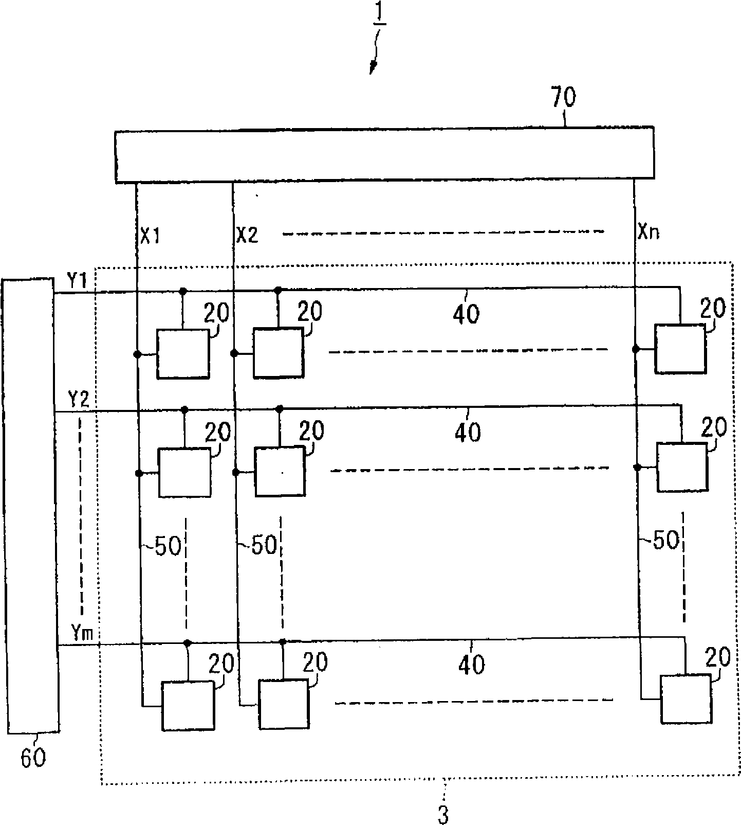
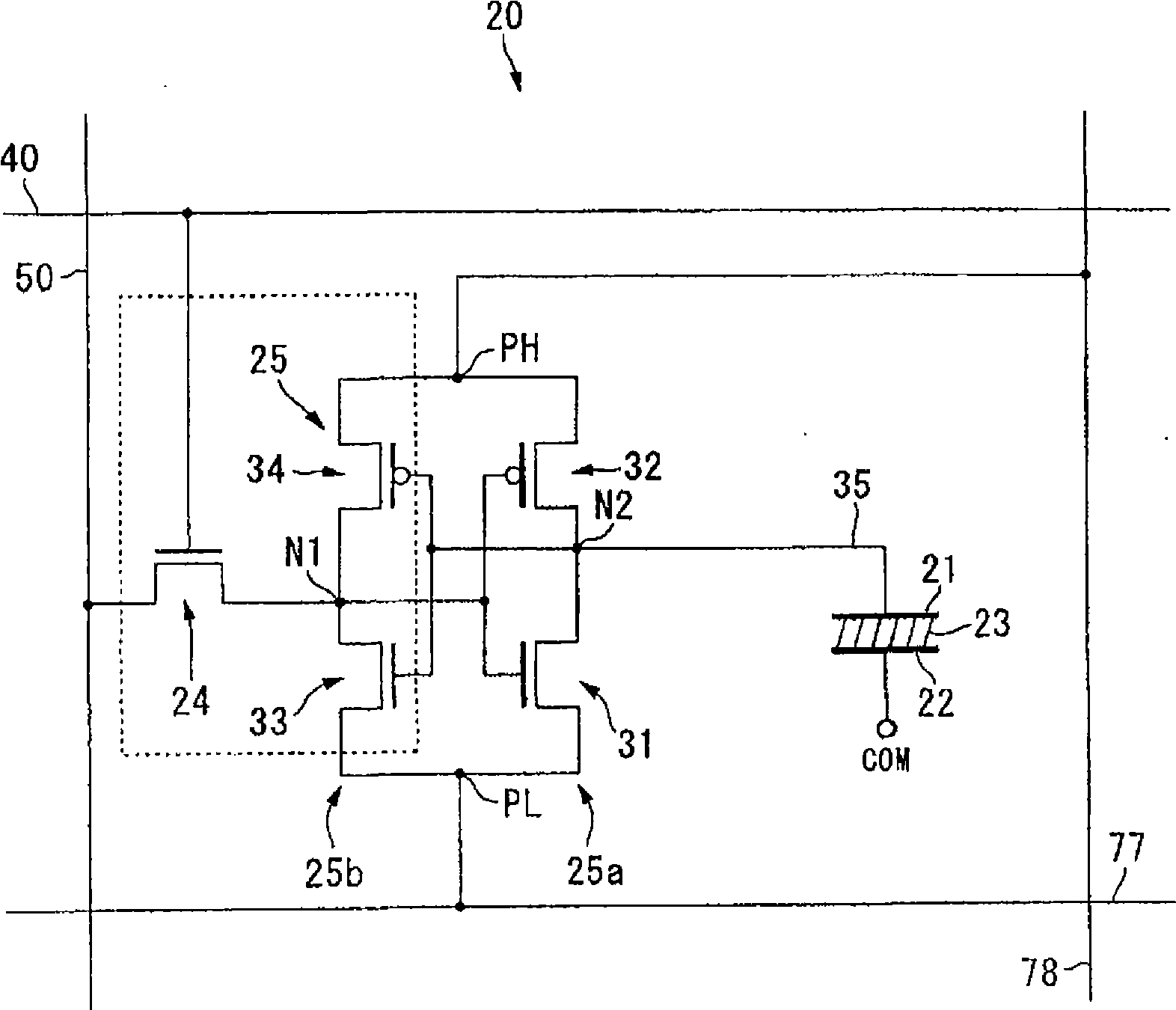
[0098] Next, Embodiment 2 of the present invention will be described. The configuration of the electrophoretic display device 101 of the present embodiment is similar to that of the first embodiment. figure 2 and Figure 5 In the pixel 20 shown, an inverted data line and a selection transistor connected to the inverted data line are provided. Therefore, in the drawings to be referred to below, for those with figure 2 and Figure 5 Components that are common to the pixels 20 are assigned the same reference numerals, and their detailed descriptions are omitted.
[0099] Figure 7 The circuit configuration of the pixel 120 of the electrophoretic display device 101 is shown, which is the same as that of Embodiment 1. figure 2 Corresponding.
[0100] Such as Figure 7 As shown, the pixel 120 includes a selection transistor 24 , a selection transistor 24R, a latch circuit (storage circuit) 25 , a pixel electrode 21 , a common electrode 22 and an electrophoretic element 23 ...
Embodiment approach 3
[0124] Next, Embodiment 3 of the present invention will be described. The configuration of the electrophoretic display device 201 of the present embodiment is similar to that of the first embodiment. figure 2 In the pixel 20 shown, a transfer gate is provided as a switching circuit for potential control. Therefore, in the drawings to be referred to below, for those with figure 2 Components that are the same as those of the pixels 20 are given the same reference numerals, and their detailed descriptions are omitted.
[0125] Figure 9 The circuit configuration of the pixel 220 of the electrophoretic display device 201 is shown, which is the same as that of Embodiment 1. figure 2 Corresponding.
[0126] Such as Figure 9 As shown, the pixel 220 includes a selection transistor 24 , a latch circuit (storage circuit) 25 , transmission gates TG1 and TG2 as potential control switching circuits, a pixel electrode 21 , a common electrode 22 , and an electrophoretic element 23 . ...
Embodiment approach 4
[0144] Next, Embodiment 4 of the present invention will be described. The configuration of the electrophoretic display device 301 of the present embodiment is similar to that of the third embodiment. Figure 9 In the pixel 220 shown, an inverted data line and a selection transistor connected to the inverted data line are provided. Therefore, in the drawings to be referred to below, for those with Figure 9 Components that are the same as those of the pixels 220 are given the same reference numerals, and their detailed descriptions are omitted.
[0145] Figure 11 The circuit configuration of the pixel 320 of the electrophoretic display device 301 is shown, which is the same as that of the third embodiment. Figure 9 Corresponding.
[0146] Such as Figure 11 As shown, the pixel 320 includes a selection transistor 24 , a selection transistor 24R, a latch circuit (storage circuit) 25 , transmission gates TG1 and TG2 as potential control switching circuits, a pixel electrode 21...
PUM
 Abstract
Description
Claims
Application Information
 - R&D
- Intellectual Property
- Life Sciences
- Materials
- Tech Scout
- Unparalleled Data Quality
- Higher Quality Content
- 60% Fewer Hallucinations
Browse by: Latest US Patents, China's latest patents, Technical Efficacy Thesaurus, Application Domain, Technology Topic, Popular Technical Reports.
© 2025 PatSnap. All rights reserved.Legal|Privacy policy|Modern Slavery Act Transparency Statement|Sitemap|About US| Contact US: help@patsnap.com


