Structure for sensing wafer, wafer-class sensing assembling structure and method for producing same

A manufacturing method and a technology for sensing chips, which are applied in radiation control devices, semiconductor/solid-state device manufacturing, electrical components, etc., can solve problems such as inability to actuate, deteriorate, and change, and achieve the effect of reducing the size of the structure

Inactive Publication Date: 2012-08-22
IND TECH RES INST
View PDF4 Cites 0 Cited by
  • Summary
  • Abstract
  • Description
  • Claims
  • Application Information

AI Technical Summary

Problems solved by technology

Since the stress release layer 11 above the conventional semiconductor wafer 10 covers the entire surface of the wafer 10 except the chip bonding pad 12 area, the fabrication of the conductive metal layer 14 loaded with the patterned photoresist 13 The method does not come into contact with the surface of the chips on the wafer 10, but this technique is applied on a sensing wafer with open spaces, each sensing chip has a sensing area in it, and its sensing area is in the entire In the fabrication method of structuring, it is necessary to maintain communication with the outside world, that is to say, for the stress release layer in the fabrication method of wafer level structuring, for the sensing wafer, in addition to the chip bonding pad area, it must also be on the surface of each chip. The sensing area has a design that must not be covered, otherwise, in the subsequent manufacturing method of loading the conductive metal layer of the whole wafer, the loaded metal will also be loaded on the sensing area of ​​each sensing chip on the wafer at the same time, so the sensing layer material Contamination or changes in the sensing design lead to the failure, attenuation, deterioration or failure of the sensing function of the sensing layer

Method used


Image

  • Structure for sensing wafer, wafer-class sensing assembling structure and method for producing same
  • Structure for sensing wafer, wafer-class sensing assembling structure and method for producing same
  • Structure for sensing wafer, wafer-class sensing assembling structure and method for producing same

Examples


Embodiment Construction

[0031] The preferred embodiments of the present invention are described in detail as follows in conjunction with the accompanying drawings.

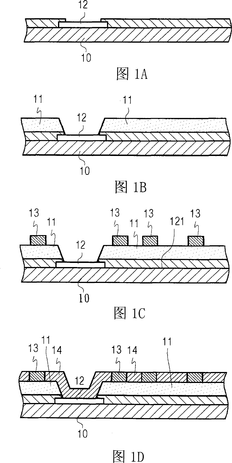
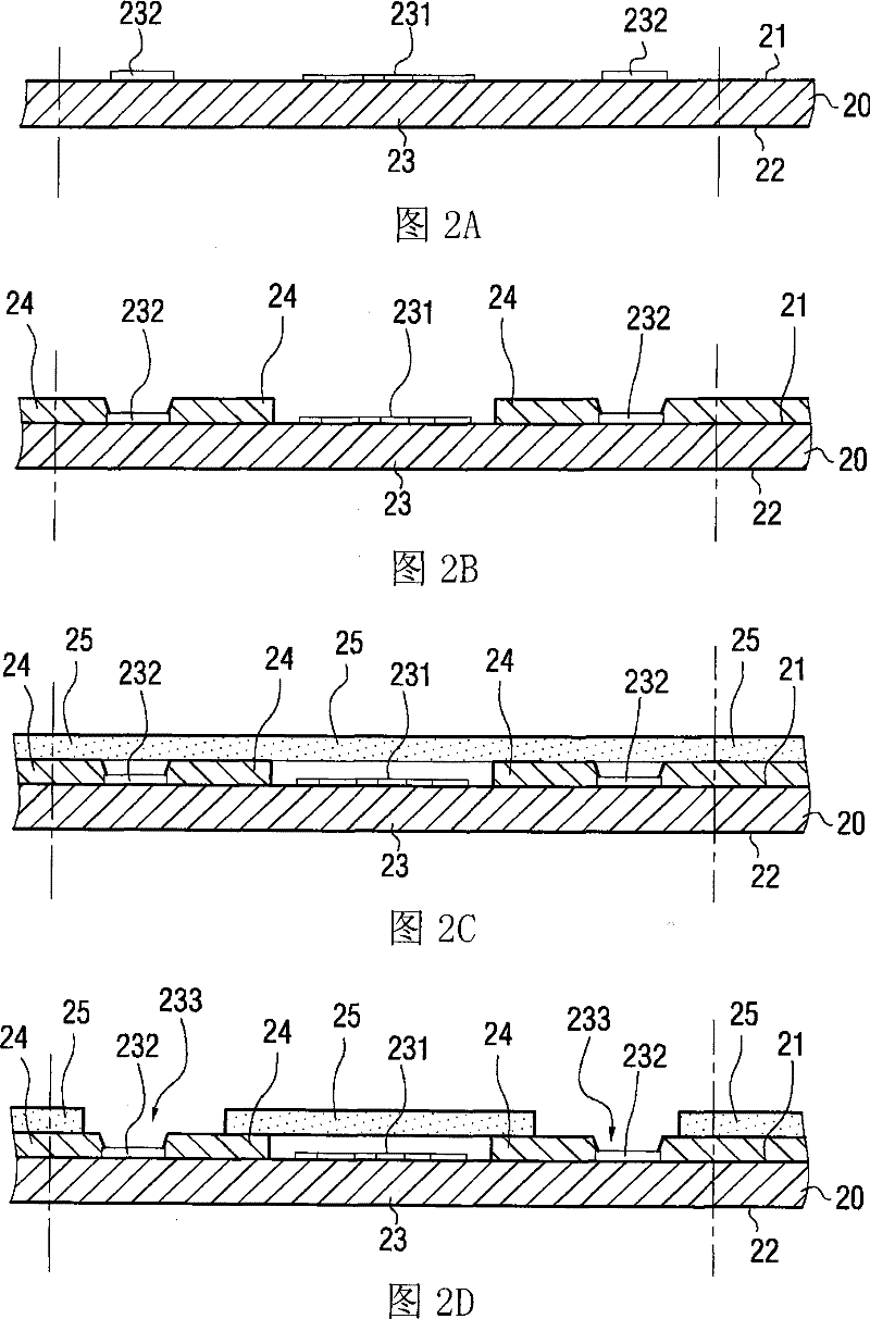
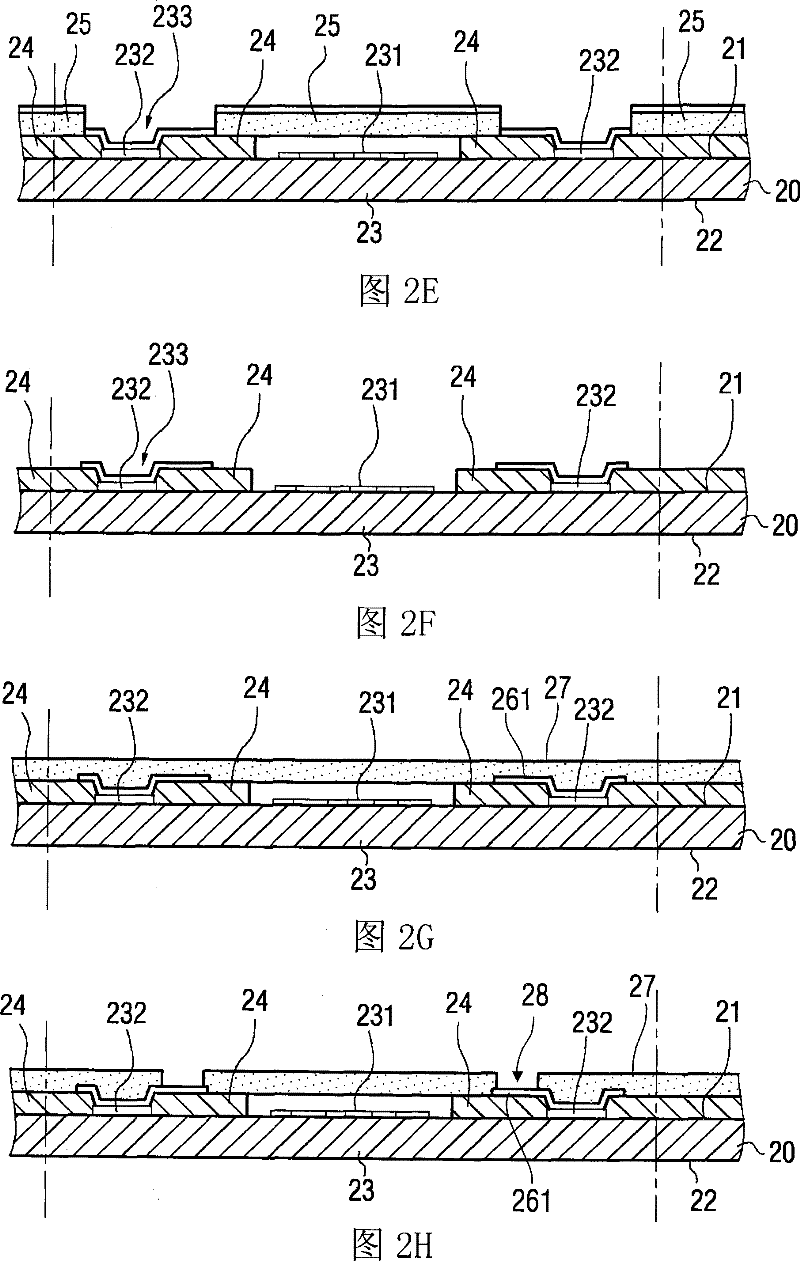
[0032] see Figure 2A and Figure 2K A schematic structural flow diagram of an embodiment of the fabrication method of the wafer-level sensing assembly structure of the present invention is shown. It comprises the following steps: first provide a chip 20, especially a sensing chip, the chip 20 is made up of a plurality of sensing chips 23, the chip 20 has a chip surface 21 and the opposite chip back 22, each chip on the chip surface 21 The sensing chip 23 includes a sensing region 231 and a plurality of bonding pads 232 ( Figure 2A shown). Then form a stress release layer 24 on the wafer surface 21 (it is mainly used for force buffering, and is often called a stress buffer layer), and its stress release layer 24 exposes the sensing region 231 and the welding pad 232 of the sensor chip 23 ( Figure 2B shown). Then coat a photoresist...


PUM


Abstract

The invention discloses a structure for a sensing wafer, a wafer-class sensing assembling structure and a method for producing the same. The method comprising the following steps that: a wafer including a sensing chip is provided, and the sensing chip comprises a sensing region and a welding pad; a stress relief layer is formed on the surface of the wafer; a photoresistive layer is covered on the stress relief layer; a photoresist layer is patternized so as to expose the welding pad and partial stress relief layer but not to expose an opening region of the sensing region; a conducting metal layer for re-distributing the welding pad is formed on the stress relief layer not covered by the photoresist layer; the photoresist layer is removed; a photoresist layer is re-formed on the stress relief layer and the conducting metal layer; and the re-formed photoresist layer above the re-distributing welding region is opened to form an opening; and a conducting convex block is formed on the opening so as to be electrically connected with the conducting metal layer.

Description

technical field [0001] The present invention relates to a wafer-level sensing assembly structure and fabrication method, in particular to a fabrication structure and fabrication that can protect the sensing area from contamination and reduce the volume of the assembly when the sensing wafer is rewired. method. Background technique [0002] As far as the current micro-electro-mechanical industry is concerned, although micro-electro-mechanical components are born with the characteristics of miniaturization and integrated integration, because the overall component cost has always been high, the field and scope of its components will be greatly reduced. With the trend of personalization and popularization of global communications, it is not uncommon for everyone to own a mobile phone or own a mobile phone. Even elementary school children who have just started school, because of the need for parent-child contact, the age of mobile phone consumer groups , significantly reduced to...

Claims


Application Information

Patent Timeline
Patent Type & Authority Patents(China)
IPC IPC(8): H01L27/144H01L23/485H01L21/60
CPCH01L2224/13
Inventor 陈荣泰朱俊勋何宗哲蔡伯晨
Owner IND TECH RES INST
Why Eureka
Try Eureka