Layout capable of weightily welding pad and debug method applying the same
A technology that can be reworked and reworked, used in the direction of electrical connection of printed components, secondary processing of printed circuits, printed circuit components, etc.
- Summary
- Abstract
- Description
- Claims
- Application Information
AI Technical Summary
Problems solved by technology
Method used
Image
Examples
Embodiment Construction
[0020] The spirit of the present invention will be clearly described below in conjunction with the accompanying drawings and detailed descriptions. Any person with ordinary knowledge in the technical field can change and modify the technology implied by the present invention after understanding the preferred embodiments of the present invention. without departing from the spirit and scope of the present invention.
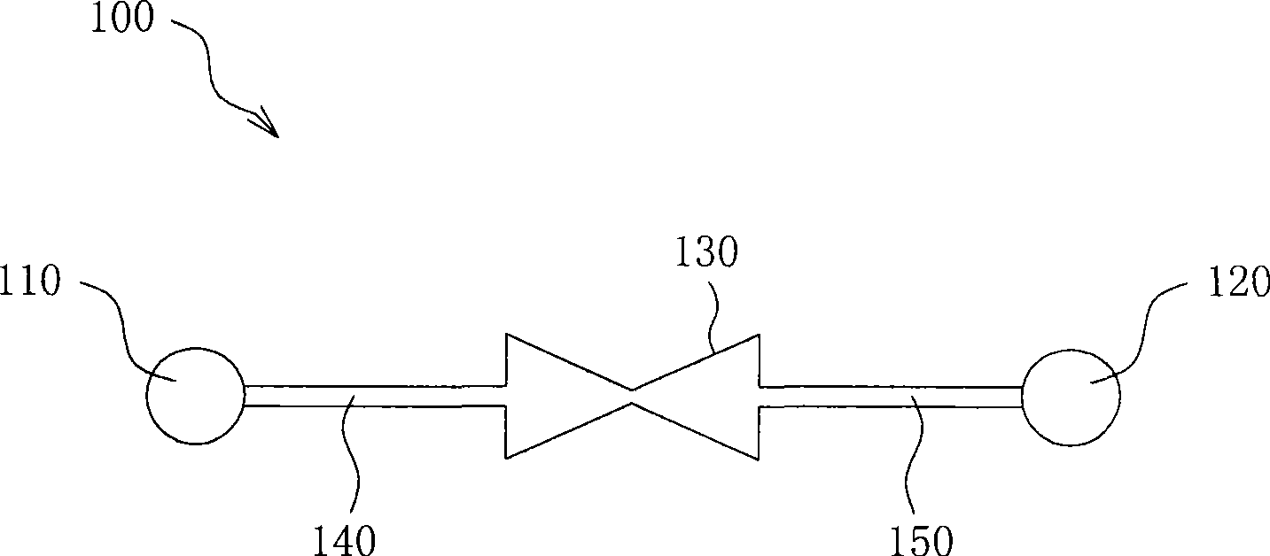
[0021] refer to figure 1 , shows a schematic diagram of a preferred embodiment of the reworkable pad layout of the present invention. The reworkable pad layout 100 can be applied in the debugging process of a circuit board, especially for replacing the traditional zero-ohm resistor in the debugging process. The reworkable pad layout 100 includes a first terminal 110 , a second terminal 120 , and a reworkable pad 130 . During the circuit design stage of the circuit board, a debug location may be reserved between the first terminal 110 and the second terminal 120 ,...
PUM
 Abstract
Description
Claims
Application Information
 - R&D
- Intellectual Property
- Life Sciences
- Materials
- Tech Scout
- Unparalleled Data Quality
- Higher Quality Content
- 60% Fewer Hallucinations
Browse by: Latest US Patents, China's latest patents, Technical Efficacy Thesaurus, Application Domain, Technology Topic, Popular Technical Reports.
© 2025 PatSnap. All rights reserved.Legal|Privacy policy|Modern Slavery Act Transparency Statement|Sitemap|About US| Contact US: help@patsnap.com


