Pad-welding structure and debug method applying the same
A solder pad, solder technology, applied in the field of reworkable solder pads
- Summary
- Abstract
- Description
- Claims
- Application Information
AI Technical Summary
Problems solved by technology
Method used
Image
Examples
Embodiment Construction
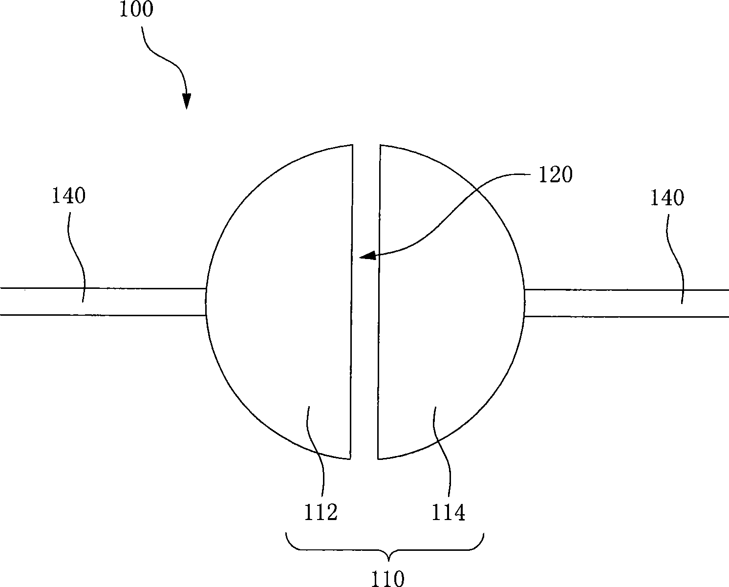
[0021] refer to figure 1 , which shows a schematic diagram of a preferred embodiment of the pad structure of the present invention. The pad structure 100 includes a pad body 110 and a blank spacer 120 . The blank spacer 120 passes through the pad body 110 to divide the pad body 110 into a primary bonding pad 112 and a secondary bonding pad 114 . Wherein, the blank spacer 120 is located between the first bonding pad 112 and the second bonding pad 114 .
[0022] Since the first welding pad 112 and the second welding pad 114 are separated by a blank spacer 120, the two cannot be connected. At this time, the main body 110 of the welding pad can be regarded as an open circuit, and the debugging step of the circuit board is performed. , the first bonding pad 112 and the second bonding pad 114 can be used as endpoints of the test respectively.
[0023] The first bonding pad 112 and the second bonding pad 114 can be part of the complete outline of the bonding pad body 110 . For ex...
PUM
 Abstract
Description
Claims
Application Information
 - R&D
- Intellectual Property
- Life Sciences
- Materials
- Tech Scout
- Unparalleled Data Quality
- Higher Quality Content
- 60% Fewer Hallucinations
Browse by: Latest US Patents, China's latest patents, Technical Efficacy Thesaurus, Application Domain, Technology Topic, Popular Technical Reports.
© 2025 PatSnap. All rights reserved.Legal|Privacy policy|Modern Slavery Act Transparency Statement|Sitemap|About US| Contact US: help@patsnap.com


