
Liquid crystal display panel, liquid crystal display device and method for manufacturing liquid crystal display panel

A liquid crystal display panel and display area technology, applied in nonlinear optics, instruments, optics, etc., can solve the problems of display image quality error, increase in proportion, increase in hygroscopicity, etc.

Inactive Publication Date: 2009-06-17
KYOCERA CORP
View PDF2 Cites 11 Cited by
  • Summary
  • Abstract
  • Description
  • Claims
  • Application Information

AI Technical Summary

Problems solved by technology

[0008] However, in the transflective liquid crystal display device disclosed in Patent Document 2, the color filter is formed in a portion where no reflective film is formed, and if the color filter is not formed on the reflective film, due to the The thickness (for example, 1 to 2 μm) is larger than the thickness of the reflective film (for example, 0.1 μm), so there will be a large step difference between the two (a step difference that cannot be absorbed by a general planarizing film)
If such a step difference occurs, a large error will occur in the thickness (Gap) of the liquid crystal layer existing between the substrate electrodes, so if the display characteristics of a display method such as one of a transmissive display method and a reflective display method If optimized, the contrast ratio and other characteristics of the other display method will be reduced
In addition, in order to reduce the influence of a large level difference, if the film thickness of the planarization film is increased beyond the general range, the four problems shown below may occur
First, as the film thickness of the planarizing film increases, it becomes difficult to ensure the uniformity of the film thickness of the planarizing film itself, and as a result, an error occurs in the image quality of the displayed image
Second, by increasing the film thickness of the planarizing film, which is usually about 2 to 3 μm in thickness, the amount of penetration into the planarizing film by the spacer (particle size: about 4 to 6 μm) which is higher in hardness than the planarizing film may sometimes be reduced. Big
In this way, if the amount of penetration becomes large, errors are likely to occur in the cell gap, and the driving voltage will fluctuate.
Third, since the planarizing film is usually made of acrylic resin, the increase in the ratio of its presence increases the hygroscopicity and deteriorates the liquid crystal characteristics.
Fourth, increase in cost or weight due to increase in usage of planarizing film
In addition, Patent Document 2 also discloses a transflective liquid crystal display device composed of a reflective film having a light passage hole formed on a color filter formed on the entire substrate in order to reduce the influence of the above-mentioned level difference. The over-type liquid crystal display device still has the problem that monochrome display and color display cannot be realized at the same time in the reflective display method

Method used


Image

  • Liquid crystal display panel, liquid crystal display device and method for manufacturing liquid crystal display panel
  • Liquid crystal display panel, liquid crystal display device and method for manufacturing liquid crystal display panel
  • Liquid crystal display panel, liquid crystal display device and method for manufacturing liquid crystal display panel

Examples


Embodiment Construction

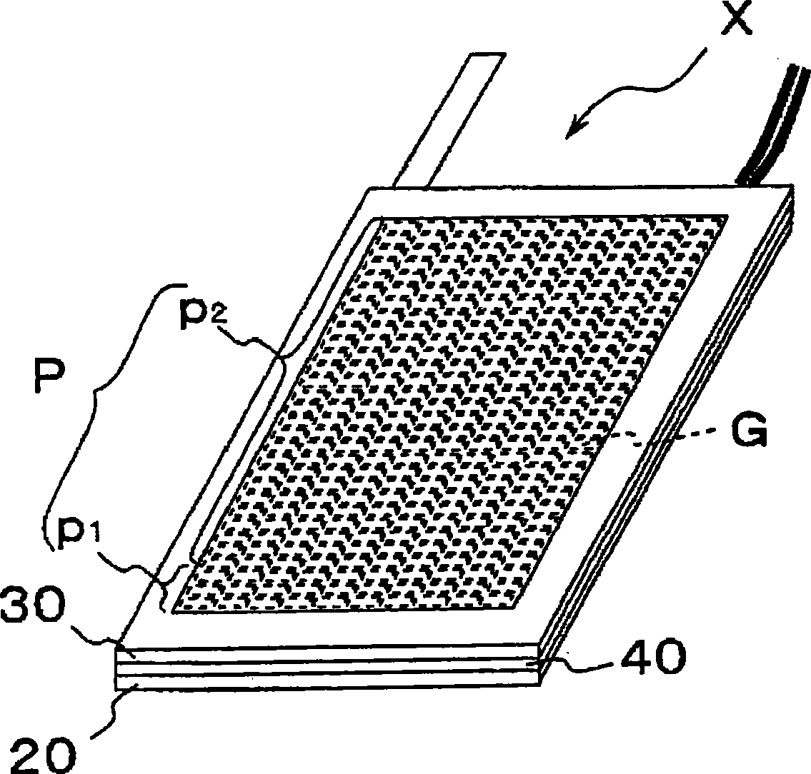
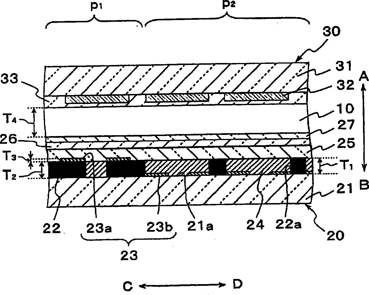
[0052] figure 1 It is a perspective view showing a schematic configuration of a transflective liquid crystal display panel X according to an embodiment of the present invention. figure 2 Yes figure 1 An enlarged cross-sectional view of main parts of the liquid crystal display panel X shown.

[0053] The liquid crystal display panel X includes a liquid crystal layer 10, a first base 20, a second base 30, and a sealing member 40. By interposing the liquid crystal layer between the first base 20 and the second base 30, the liquid crystal layer 10 is sealed by the sealing member 40. , thereby forming a display area P including a plurality of pixels G for displaying images.

[0054] The liquid crystal layer 10 exhibits electronic, optical, mechanical, or magnetic anisotropy, and is a layer composed of liquid crystals that have both solid regularity and liquid fluidity. As the liquid crystal, nematic liquid crystal, color-changing liquid crystal, smectic liquid crystal, etc. are...


PUM

PropertyMeasurementUnit
particle diameteraaaaaaaaaa

Abstract

A liquid crystal display panel, a liquid crystal display device and a manufacturing method of a liquid crystal display, which have excellent display properties and achieve high color purity in a transmissive display mode and high display brightness in monochrome display in a reflective display mode, are provided. A liquid crystal display panel X according to one of the present invention includes: a first base (20) having a display-area portion p 1 that includes a transparent substrate (21), a light shielding film (22) formed on a main surface of the transparent substrate (21) and having through holes, a light reflecting film (23) formed on the light shielding film (22), a color filter (24) formed on the main surface of the transparent substrate (21) exposed in the through holes of the light shielding film (22), and a transparent electrode (26) formed on the main surface of the transparent substrate (21); a second base (30) that includes a transparent substrate (31), and a transparent electrode (32) formed on a main surface of the transparent substrate (31); and a sealing member (40) for sealing liquid crystal between the first base (20) and the second base (30).

Description

technical field [0001] The present invention relates to a so-called transflective liquid crystal display panel including, among a plurality of pixels constituting a display area, a transmission area configured to transmit light from a backlight, for example, and a reflection area configured to reflect external light, and A liquid crystal display device, and a method for manufacturing a liquid crystal display panel. Background technique [0002] In recent years, liquid crystal display devices equipped with liquid crystal display panels have become popular not only in relatively small information communication equipment such as portable information terminals, but also in relatively large electrical equipment such as monitors. In order to reduce power consumption, a reflective liquid crystal display device that does not require a backlight is adopted. However, since reflective liquid crystal display devices use external light (such as sunlight) as a light source, it tends to b...

Claims


Application Information

Patent Timeline
Patent Type & Authority Applications(China)
IPC IPC(8): G02F1/1335
CPCG02F1/133512G02F1/133555G02F1/133514G02F2001/133391G02F2001/133626G02F1/133391G02F1/133626G02F1/1335G02F1/1339
Inventor 宫崎吉雄土田克巳
Owner KYOCERA CORP
Learn More