Parameter computation method of RFCMOS model with expandability
A parameter calculation and model technology, applied in the direction of calculation, electrical digital data processing, special data processing applications, etc., can solve the problems of poor scalability and achieve the effects of improving model accuracy, achieving scalability, and reducing design costs
Active Publication Date: 2010-09-08
SHANGHAI HUAHONG GRACE SEMICON MFG CORP
View PDF0 Cites 0 Cited by
- Summary
- Abstract
- Description
- Claims
- Application Information
AI Technical Summary
Problems solved by technology
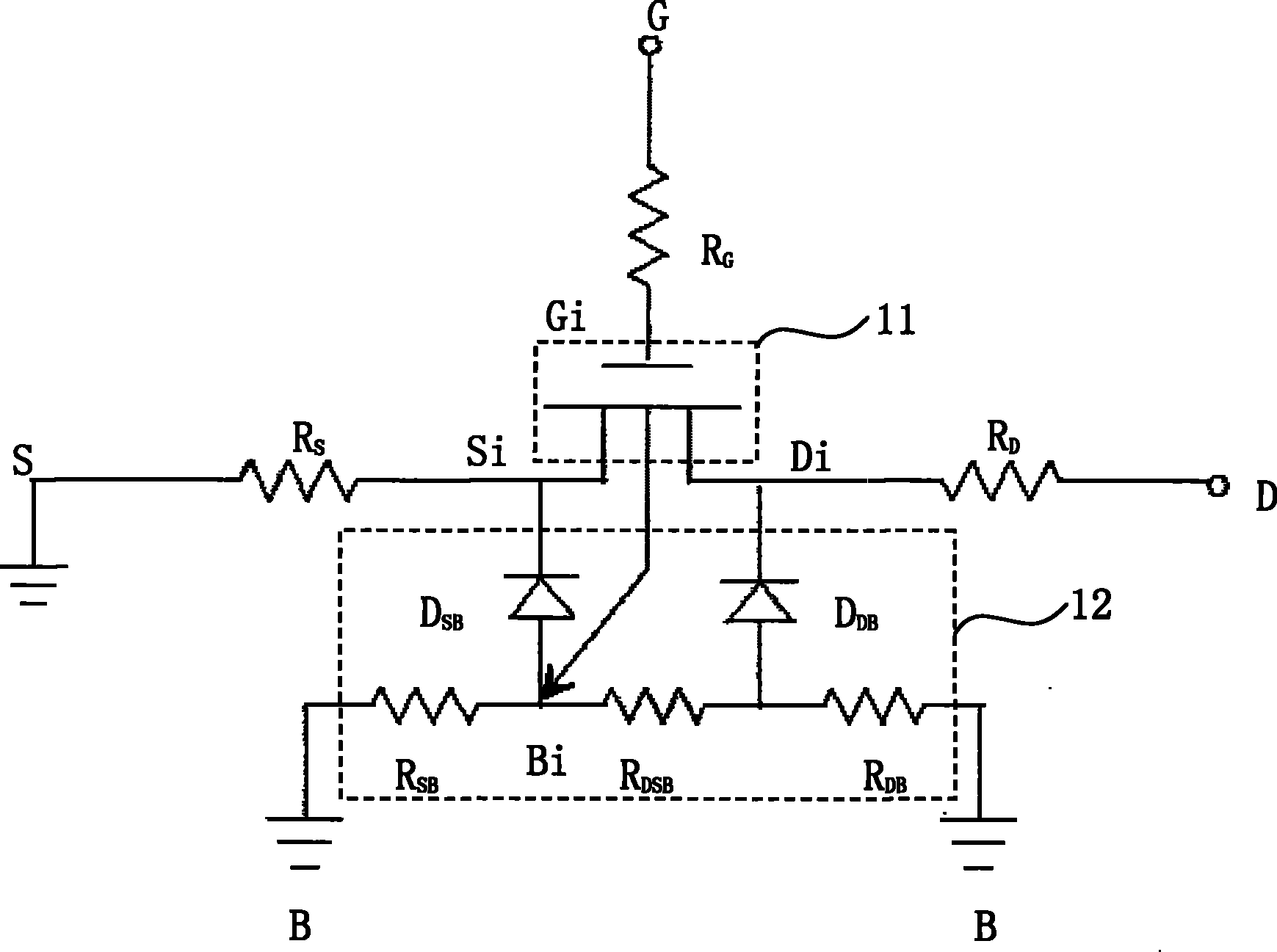
Due to the particularity of RFCMOS layout design, most of the RFCMOS models shown in Figure 1 are limited to simulating RFCMOS devices of a certain size or a small range of sizes, and the scalability is poor.
Method used
View moreImage
Smart ImageViewing Examples

Examples
Embodiment Construction
Login to View More PUM
 Abstract
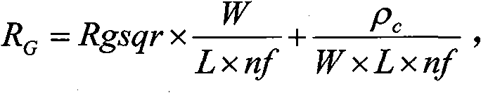
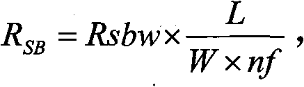
The invention discloses a parameter calculation method for RFCMOS models of expansibility. The model adds a sub circuit based on the MOS field transistor of BSIM3V3 model, wherein the sub circuit comprises a parasitic resistance of grid electrode, a parasitic resistance of source electrode, a parasitic resistance of drain electrode and a substrate network. The substrate network comprises a parasitic diode between the source electrode and the substrate, a parasitic diode between the drain electrode and the substrate, a coupling resistance between the source electrode and the substrate, a coupling resistance between the drain electrode and the substrate, and a coupling resistance of the substrate. The parasitic resistance of the grid electrode and the components forming the substrate network are calculated from variable parameters which at least comprise one of transistor channel length, channel width and the number of parallel grid electrodes. The parameter calculation method improves model precision, effectively realizes model expansibility and effectively reduces the design cost of radio frequency circuits.
Description
technical field The present invention relates to an RFCMOS (Radio Frequency CMOS) model. Background technique With the continuous development of CMOS technology, deep submicron CMOS devices have the characteristics of high-frequency signal transmission and low noise, so they are more and more used in radio frequency (RF) circuit design and widely used in the field of wireless communication. In RFCMOS circuit design, only by establishing an accurate RFCMOS model can the performance of RFCMOS devices be accurately simulated during circuit simulation, thereby saving the RFCMOS circuit design cycle. The RFCMOS model requires more emphasis on describing high-frequency performance such as nonlinearity, high-frequency noise, and non-quasi-static effects of RFCMOS devices on the basis of including all low-frequency characteristics. So far, there is no standard RFCMOS model in the industry, and RFCMOS devices are usually simulated by adding branch circuits based on the BSIM3v3 mod...
Claims
Login to View More Application Information
Patent Timeline
 Patent Type & Authority Patents(China)
IPC IPC(8): G06F17/50
Inventor 武洁李平梁
Owner SHANGHAI HUAHONG GRACE SEMICON MFG CORP
Features
- R&D
- Intellectual Property
- Life Sciences
- Materials
- Tech Scout
- Unparalleled Data Quality
- Higher Quality Content
- 60% Fewer Hallucinations
Learn More Browse by: Latest US Patents, China's latest patents, Technical Efficacy Thesaurus, Application Domain, Technology Topic, Popular Technical Reports.
© 2025 PatSnap. All rights reserved.Legal|Privacy policy|Modern Slavery Act Transparency Statement|Sitemap|About US| Contact US: help@patsnap.com