
Capacitance type touch control screen and manufacturing method thereof

A technology of capacitive touch and processing method, which is applied in the direction of electric digital data processing, instrument, data processing input/output process, etc., can solve the problems of processing inconvenience, and achieve convenient processing, improved brightness and contrast, and low consumables Effect

Inactive Publication Date: 2009-05-27
CSG HOLDING
View PDF0 Cites 84 Cited by
  • Summary
  • Abstract
  • Description
  • Claims
  • Application Information

AI Technical Summary

Problems solved by technology

[0006] The technical problem to be solved by the present invention is to provide a method for providing a film layer only on one side of the substrate in view of the problem that the film layer needs to be processed on both sides of the substrate in the capacitive touch screen in the prior art and the processing is inconvenient. capacitive touch screen

Method used


Image

  • Capacitance type touch control screen and manufacturing method thereof
  • Capacitance type touch control screen and manufacturing method thereof
  • Capacitance type touch control screen and manufacturing method thereof

Examples


Embodiment Construction

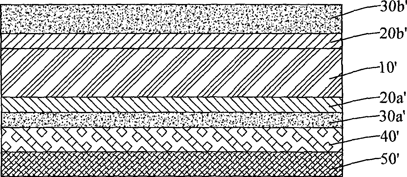
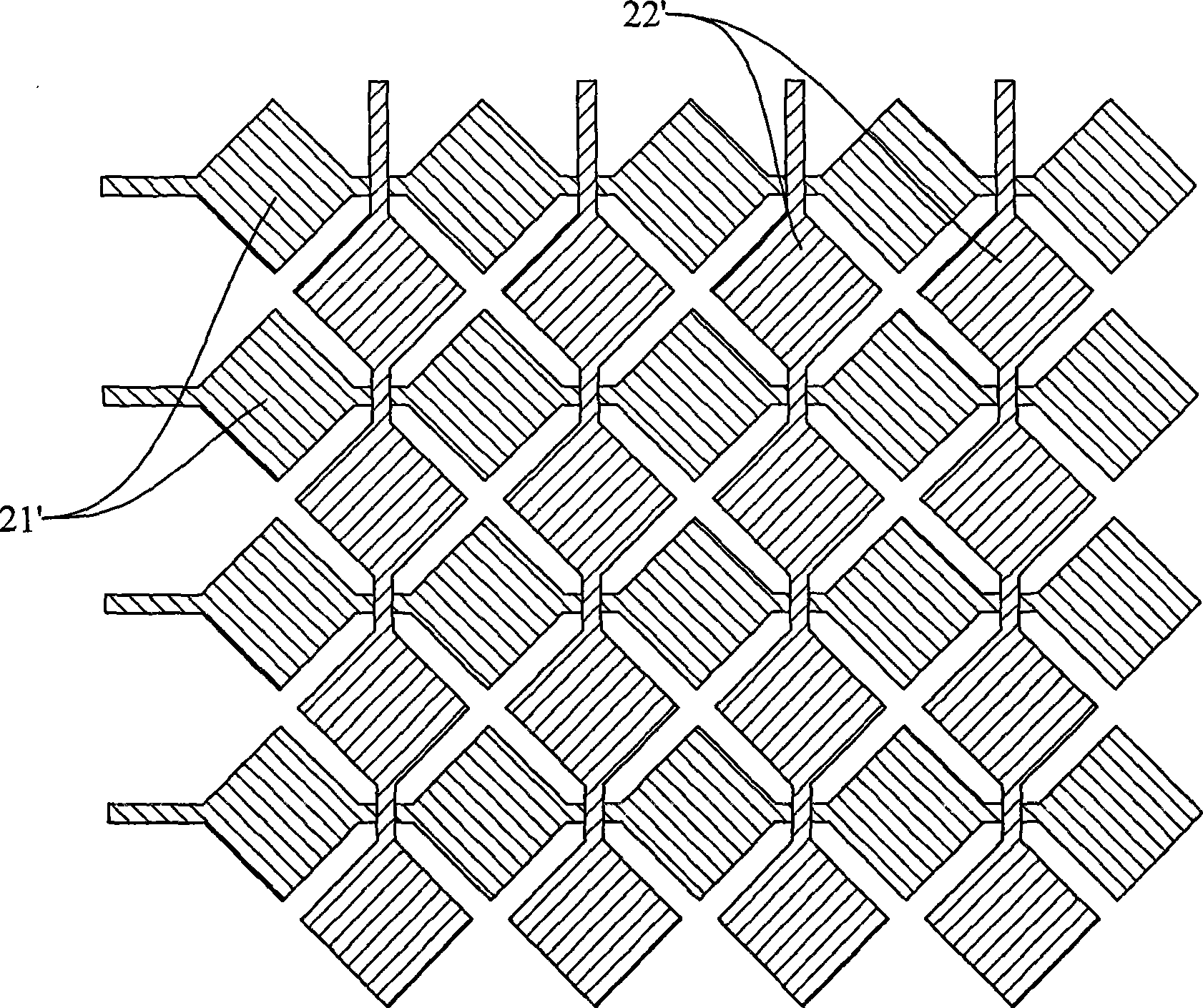
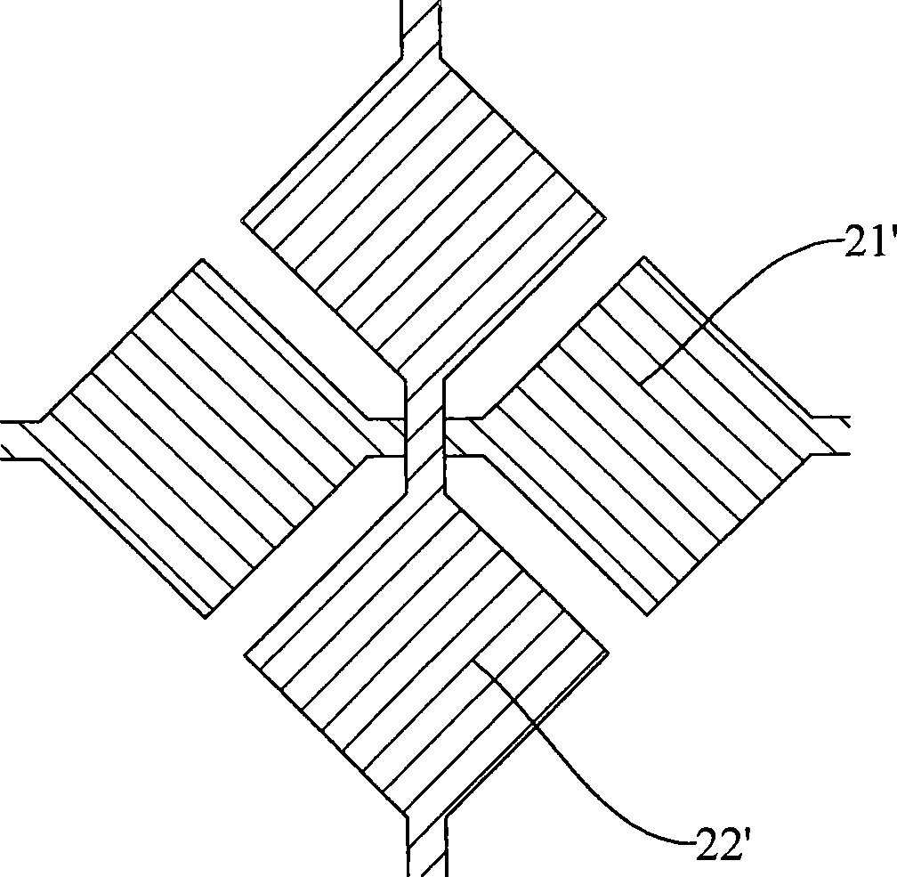
[0057] Such as Figure 4 As shown, in the first embodiment of the capacitive touch screen of the present invention, it includes a substrate 10 , an ITO (Indium Tin Oxide, indium tin oxide) layer 20 , an insulating layer 30 , a circuit layer 40 and a protective layer 50 . Among them, the substrate 10 is mostly made of tempered glass, etc., the ITO layer 20 is formed by a plurality of first axis traces 21 and second axis traces 22 , the insulating layer 30 is disposed on the ITO layer 20 , and the circuit layer 40 is disposed on the insulating layer 30 . Such as Figure 5 As shown, a plurality of first axis traces 21 are arranged parallel to each other, a plurality of second axis traces 22 are arranged parallel to each other, and the first axis traces 21 and the second axis traces 22 intersect to form the ITO layer 20 . Such as Image 6 , 7 As shown, at the intersection, the first axis trace 21 is divided into a plurality of units P by the second axis trace 22, and two adjace...


PUM


Abstract

The invention relates to a capacitive touch screen, which comprises a substrate and an ITO layer, an insulating layer, a circuit layer and a protective layer which are arranged on the same side with the substrate, wherein the ITO layer consists of various mutually parallel first axial traces and various mutually parallel second axial traces which are intersected; the first axial traces and the second axial traces are perpendicular to each other; each first axial trace is separated into various units by various second axial traces which are intersected with the first axial trace; two adjacent units in the same first axial trace are electrically connected through metal bridges; and insulating pieces for insulating the metal bridges and the second axial traces are arranged between the metal bridges and the second axial traces. Because the ITO layer which simultaneously comprises the first axial traces and the second axial traces is arranged on the same side with the substrate, the thickness of the whole film layer is thinned; the structure of the whole touch screen is simplified; the manufacturing cost is reduced; and the transmittance of the touch screen is improved. The invention also discloses a processing method for manufacturing the capacitive touch screen.

Description

【Technical field】 [0001] The present invention relates to a capacitive touch screen, and more specifically, to a capacitive touch screen and a manufacturing method of the capacitive touch screen. 【Background technique】 [0002] Touch screens have been widely used in various electronic products. The user can touch the screen with a finger or a special pen to generate a change in electrical signal, and then recognize and select the text, symbols, menus, etc. displayed on the display device behind the touch screen to realize the input operation of the device. [0003] Touch screens are generally divided into resistive, electromagnetic and capacitive types. The working principle of capacitive touch screens is to use the current induction of the human body to work. A traditional capacitive touch screen is structured on a four-layer printed circuit board, which is a ground layer, an X-axis trace, a Y-axis trace, and a circuit layer. Such a capacitive touch screen is expensive to...

Claims


Application Information

Patent Timeline
IPC IPC(8): G06F3/044
Inventor 何强民毛利良刘锡刚贾文傅志敏黄受林
Owner CSG HOLDING
Learn More