A method for manufacturing an electronic assembly, electronic assembly, covering piece and substrate

A technology for electronic components and coverings, applied in the process of producing decorative surface effects, electrical components, and final product manufacturing, which can solve problems such as damage and achieve a stable and reliable support effect

Active Publication Date: 2009-04-29
盛投资有限责任公司
View PDF3 Cites 3 Cited by
  • Summary
  • Abstract
  • Description
  • Claims
  • Application Information

AI Technical Summary

Problems solved by technology

Such damage can occur, for example, when the substrate and metallization or tooling are not properly aligned

Method used


Image

  • A method for manufacturing an electronic assembly, electronic assembly, covering piece and substrate
  • A method for manufacturing an electronic assembly, electronic assembly, covering piece and substrate
  • A method for manufacturing an electronic assembly, electronic assembly, covering piece and substrate

Examples


Embodiment Construction

[0029] As previously described, like reference numerals designate like parts in the drawings.

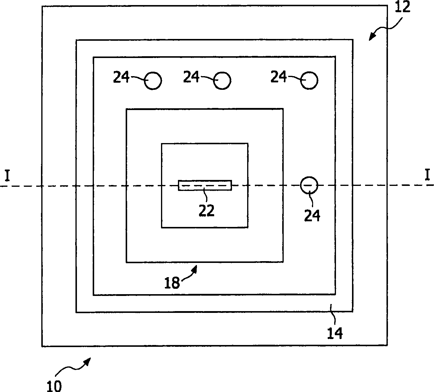
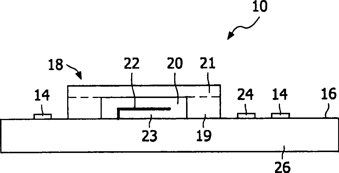
[0030] Referring now to FIGS. 1 a and 1 b , an electronic component 10 having a first pattern 12 of substantially closed structures 14 can be seen. A cover 18 is provided on the surface of the electronic component. The cover 18 together with the surface 16 defines a cavity 20 . Cavity 20 accommodates MEMS element 22 . The first pattern includes contact areas 24 electrically connected to electrical contacts of the electronic component (not shown).

[0031] As shown in FIGS. 1 a and 1 b , the closure structure 14 of the first pattern 12 seals the covering at the surface 16 . The closure structure 14 here has a rectangular shape. However, it may also have a circular, hexagonal or other suitable shape.

[0032] Preferably, the body 26 of the electronic component 10 comprises an integrated circuit, the solder pads of which are connected to the contact areas 24 . The MEMS element 22...


PUM


Abstract

The present invention relates to a method for manufacturing an electronic assembly (50) comprising an electronic component, a cavity and a substrate which method comprises; -providing an electronic component (10) having a first pattern with a substantially closed configuration; -providing a cover (18) on a surface of the electronic component, which cover together with said surface defines a cavity (20), the closed configuration of the first pattern substantially enclosing the cover at said surface; -providing a substrate (30) having a second pattern with a substantially closed configuration, which closed configuration at least partially corresponds to the closed configuration of the first pattern and comprises a solder pad; -disposing solder material at the solder pad; -positioning the electronic component and the substrate so as to align both the substantially closed configurations of the first and second pattern, while the substrate supports a top surface (28) of the cover; -reflow-soldering the solder material, therewith providing a soldered connection (52) between the first and second pattern. Furthermore the present invention relates to an electronic assembly (50), a cover (18) and a substrate (30).

Description

technical field [0001] The invention relates to a method for manufacturing an electronic component comprising an electronic component, a cavity and a substrate. Background technique [0002] Such a method is known for example from EP0951069. This document discloses the mounting of electronic components on a substrate by means of a soldering ring such that at least a part of said components is located inside the cavity. The electronic component includes microstructures, such as MEMS (micro-electromechanical systems) elements, arranged in cavities. The solder rings are on the electronic components and the corresponding metal patterns are on the substrate. The cavity is formed by aligning and bonding the solder ring to the metal pattern. The ring thus forms a closed structure, while the combination of the assembly, welded ring and substrate forms a seal. To allow removal of unwanted gases from the cavity, grooves are created in the solder ring prior to the bonding step. Al...

Claims


Application Information

Patent Timeline
IPC IPC(8): B81C1/00
CPCB81C1/00269H05K2203/1147H05K2201/10371B81C1/00833B81C2203/035H05K2201/10477H05K3/341Y10T29/49117Y02P70/50
Inventor 约翰内斯·W·维坎普康奈丽斯·斯郎布雅格布·M·舍尔弗雷克·E·范斯坦腾
Owner 盛投资有限责任公司
Why Eureka
Try Eureka