Systems and methods for forming integrated circuit components having matching geometries

A technology of integrated circuits and geometric shapes, applied in circuits, electrical components, electric solid devices, etc., can solve the problems of reducing efficiency, increasing the cost of integrated circuit devices, increasing cycle time and manpower, etc., to reduce cycle time and reduce geometry Shape difference, effect of increasing yield

Inactive Publication Date: 2009-04-22
TOPPAN PHOTOMASKS INC
View PDF0 Cites 4 Cited by
  • Summary
  • Abstract
  • Description
  • Claims
  • Application Information

AI Technical Summary

Problems solved by technology

Such handling of these components on semiconductor wafers can increase cycle time and manpower, which can reduce efficiency and thereby increase the cost of manufacturing integrated circuit devices

Method used


Image

  • Systems and methods for forming integrated circuit components having matching geometries
  • Systems and methods for forming integrated circuit components having matching geometries
  • Systems and methods for forming integrated circuit components having matching geometries

Examples


Embodiment Construction

[0018] refer to Figures 1 to 5 The present invention and its advantages are best understood by example embodiments wherein like numerals are used to indicate like and corresponding parts.

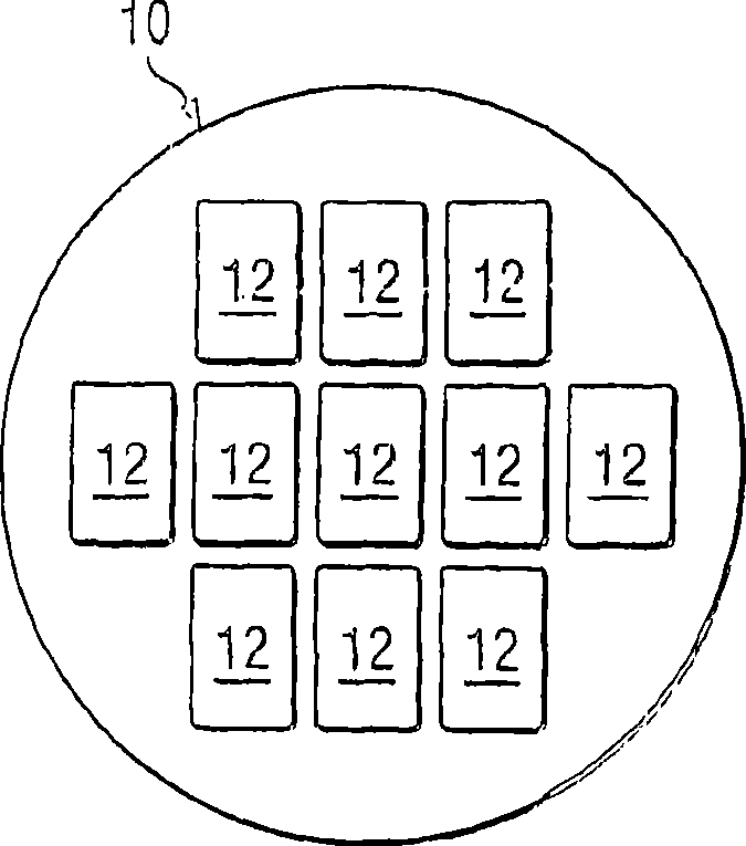
[0019] figure 1 A top view of an example semiconductor wafer 10 according to one embodiment of the invention is shown. Semiconductor wafer 10 may include a plurality of dies or chips 12, each including one or more integrated circuits including a plurality of integrated circuit components. Semiconductor wafer 10 may comprise a thin, circular sheet of monocrystalline semiconductor material suitable for use in the manufacture of semiconductor devices and / or integrated circuits. Semiconductor wafer 10 may include any suitable number of dies 12 , which may be physically separated from each other after integrated circuits are formed in each die 12 .

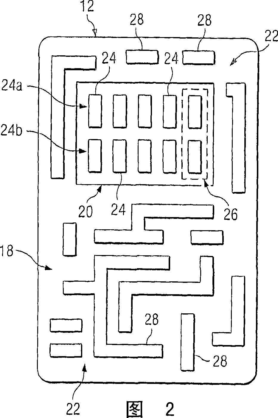
[0020] Figure 2 shows a single die 12 of a semiconductor wafer 10, which may include integrated circuit components formed in accordance with an...


PUM


Abstract

In a particular embodiment, a method of forming integrated circuit components is provided. A first photomask is formed, the first photomask including a first mask component having a first geometry corresponding to a first type of integrated circuit component. A first lithography process is performed to transfer the first geometry of the first mask component of the first photomask to a first location on a first die on a semiconductor wafer to form a first integrated circuit component of the first type of integrated circuit component on the first die. A second lithography process is performed to transfer the first geometry of the first mask component of the first photomask to a second location on the first die on the semiconductor wafer to form a second integrated circuit component of the first type of integrated circuit component on the first die.

Description

technical field [0001] The present invention relates generally to integrated circuit fabrication, and more particularly to a system and method of forming integrated circuit components with matching geometries. Background technique [0002] Integrated circuit devices typically include various circuit components, such as various transistors, resistors, and capacitors. Such integrated circuit components may be fabricated by forming specific geometries in semiconductor wafers, such as silicon wafers, using various integrated circuit fabrication techniques, such as various deposition and photolithographic techniques. In some instances, two or more electrical components of an integrated circuit device are related to each other such that characteristics of one or more of these electrical components must be "matched" in order for the integrated circuit device to function correctly or as desired. For example, it may be necessary that a particular pair of resistors in an integrated c...

Claims


Application Information

Patent Timeline
Patent Type & Authority Applications(China)
IPC IPC(8): H01L21/20
CPCH01L27/13G03F1/144H01L27/0802H01L21/32139G03F7/70466H01L27/016H01L27/0207H01L27/0805G03F1/70
Inventor K·G·格林
Owner TOPPAN PHOTOMASKS INC
Why Eureka
Try Eureka