
Active matrix substrate and display device using the same

A display device and active matrix technology, applied in identification devices, static indicators, instruments, etc., can solve problems such as inability to eliminate voltage, damage display quality, and degradation of liquid crystal 2 retention characteristics

Inactive Publication Date: 2009-04-01
SHARP KK
View PDF1 Cites 48 Cited by
  • Summary
  • Abstract
  • Description
  • Claims
  • Application Information

AI Technical Summary

Problems solved by technology

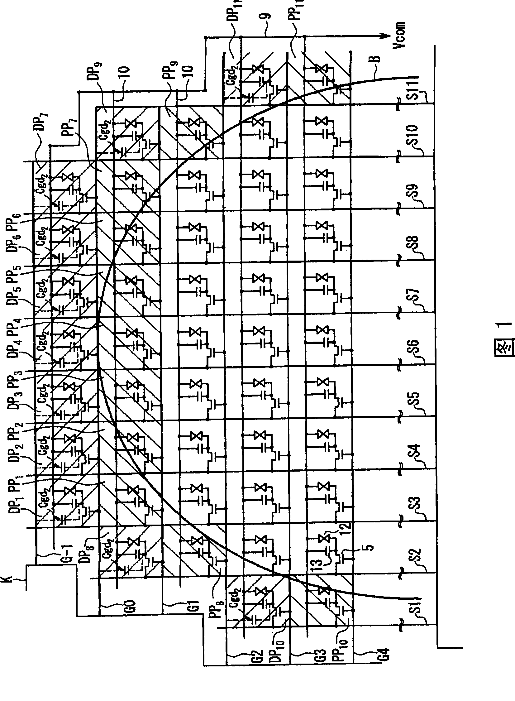
[0016] As described above, for each scan wiring G after the second level 2 , G 3 , ... are optimized to reduce the influence of the parasitic capacitance ratio α so that no DC component is applied to the liquid crystal 2, but for the uppermost scanning wiring G 1 For the corresponding pixel, because the parasitic capacitance ratio α' is different from other pixel parts, it is impossible to eliminate the variation ΔV of the voltage applied to the pixel electrode 6, so it will appear on the liquid crystal 2 of the pixel corresponding to the primary scanning line G1. apply a particularly small DC component
[0017] Moreover, if such a DC component is applied, the retention characteristics of the liquid crystal 2 will gradually deteriorate over time, and as a result, the uppermost scanning wiring G 1 For example, each pixel corresponding to one line generates a bright line at a middle gray scale in a normally white liquid crystal 2 , and a black line at a middle gray scale in a normally black liquid crystal 2 . The problem of damage to the display quality, such as (hereinafter, these phenomena are collectively referred to as bright lines, etc.)

Method used


Image

  • Active matrix substrate and display device using the same
  • Active matrix substrate and display device using the same
  • Active matrix substrate and display device using the same

Examples


Embodiment Construction

[0036] In order to achieve the above object, the active matrix substrate of the present invention is used as a substrate of a display device, which includes: a plurality of scanning wirings to which scanning signals are applied; a signal wiring; a switching element connected to the two wirings near the intersection of the scanning wiring and the signal wiring; and a pixel electrode connected to the switching element; one of the pixel electrodes corresponds to the display area of ​​the display device The distribution area of ​​the pixel electrode is in a shape other than a rectangle, and in the distribution area, at least one dummy scanning wiring is formed outside the scanning wiring at the endmost part of the scanning wiring on the scanning start side, so as to sandwich Among the outermost pixels located in the outermost periphery of the distribution area, the number of outermost pixels connected to the n-th scanning line when the scanning line at the end of the scanning line ...


PUM


Abstract

An irregular shape display device that is not rectangular in display area is provided to prevent from disadvantages of poor display dignity, and the like, due to bright lines formed by pixels at specific portions. In an active matrix substrate used as an display substrate in which a distribution region of pixel electrodes corresponding to a display region has an irregular shape other than a rectangle, at least one dummy scanning line (dummy scanning lines G0, G-1) is formed at a more outer side than a scanning line (G1) positioned at the edge portion on a scanning initiation side; and upper scanning lines are provided to extend to positions opposite to scanning lines between which a scanning line (G2) and the most outlying peripheral pixels (PP) are put and with which TFT's (5) of the most outlying peripheral pixels (PP) are connected. The dummy pixels (DP) are provided preferably at upper portions of the screen than each of the most outlying peripheral pixels (PP).

Description

technical field [0001] The present invention relates to an active matrix substrate in which switching elements such as thin film transistors are arranged in a matrix, and a display device using the active matrix substrate. Background technique [0002] Conventionally, a liquid crystal display device including an active matrix substrate in which switching elements such as thin film transistors (TFT: Thin Film Transistor) are arranged in a matrix, that is, a so-called active matrix liquid crystal display device, is known. [0003] Here, refer to Figure 6 ~ Figure 10 , the configuration of a conventional active matrix substrate and a liquid crystal display device including the substrate will be described. Figure 6 It is an equivalent circuit diagram showing the configuration of a conventional active matrix substrate. Figure 7 yes means Figure 6 A top view of the configuration of 1 pixel in the active matrix substrate. Figure 8 yes Figure 7 The A-A' line in the section...

Claims


Application Information

Patent Timeline
IPC IPC(8): G09F9/30G02F1/133G09G3/20G09G3/36
CPCG09G2300/0413G09G3/3648G09G2320/0204G02F1/134309G02F2001/133388G02F1/136286G09G3/3677G02F2201/56G02F1/133388H10K59/88
Inventor 田中信也片冈义晴今井元冈本昌也束村亲纪
Owner SHARP KK
Learn More