


Quick Research
Generate reliable direction feasibility study reports for your R&D in just a few steps.

Technical Q&A
Discover and master advanced knowledge NOW. Basics, ideas, possibilities, all at once.

Find Solutions
As an expert in R&D theories, this can generate solutions to your technical problems instantly.

Evaluate Feasibility
Analyze your overall solution with one click, know your potential R&D risks in advance.

Monitor Landscape
Get weekly tech updates, stay abreast of the latest tech innovations and key insights.
Capacitive load driving circuit and plasma display panel
A load-driven, capacitive technology, applied in the direction of static indicators, instruments, etc., can solve the problem of not being able to control odd and even numbers at the same time, to expand the negative pulse width, improve yield and reliability, and absorb panels. The effect of deviation
- Summary
- Abstract
- Description
- Claims
- Application Information
AI Technical Summary
Problems solved by technology
Method used
Image

Examples
no. 1 approach
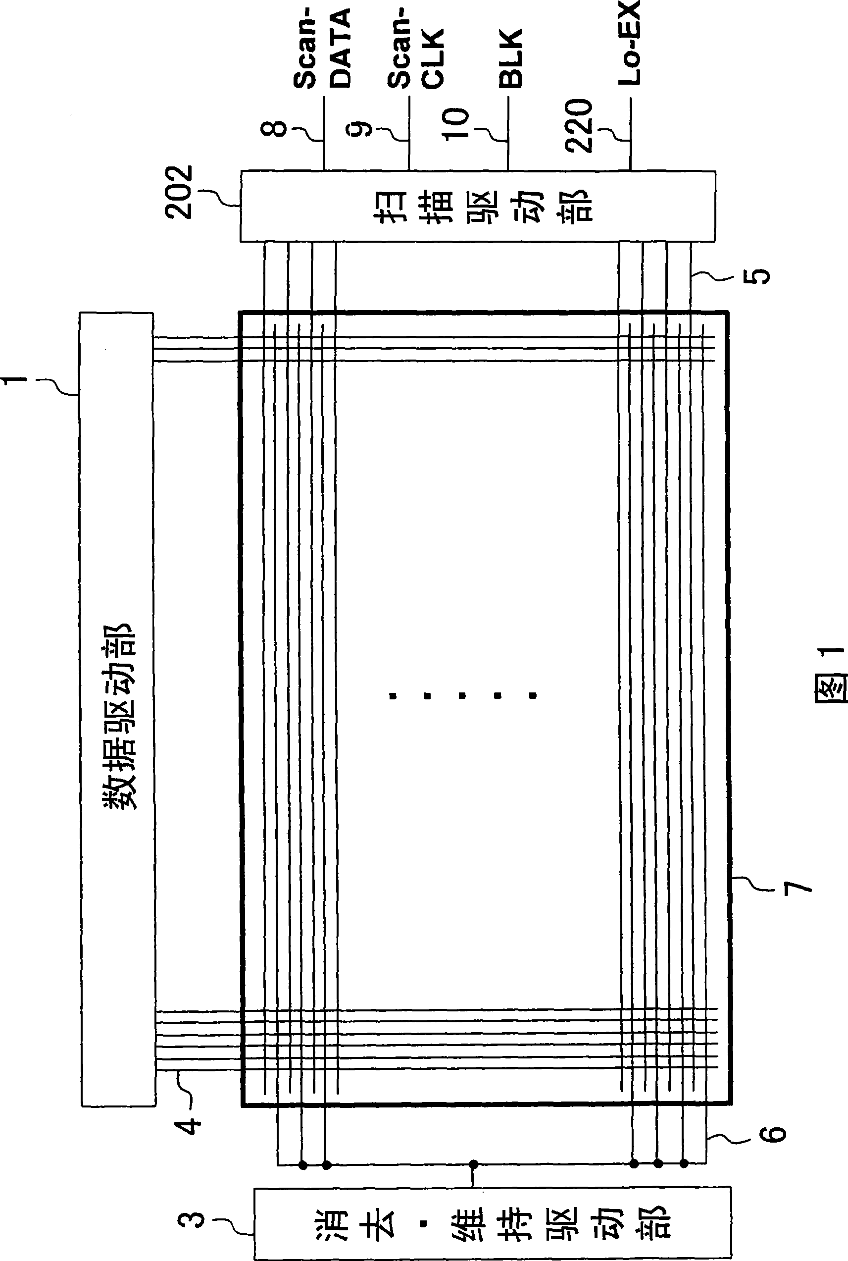
[0081] FIG. 1 is a diagram schematically showing the configuration of a PDP according to Embodiment 1 of the present invention. As shown in the figure, the PDP of this embodiment includes: a panel (display unit) 7; a plurality of data electrodes 4 arranged on the panel; a plurality of scan electrodes 5 intersecting the data electrodes 4; Erase / sustain electrode 6 provided for each scan electrode 5; scan driver 202 for driving scan electrode 5; data driver 1 for driving data electrode 4; erase / sustain driver 3 for driving erase / sustain electrode 6. Pulses having positive and negative polarities are applied to the scan electrodes 5 . In addition, components such as panel 7 , scan electrodes 5 , data electrodes 4 , and erase / sustain electrodes 6 formed on the panel serve as capacitive loads when viewed from a circuit drive unit such as scan drive unit 202 .
[0082] Scan data signal 8 , scan clock signal 9 , scan blanking signal 10 , and negative polarity pulse width control sig...
no. 2 approach
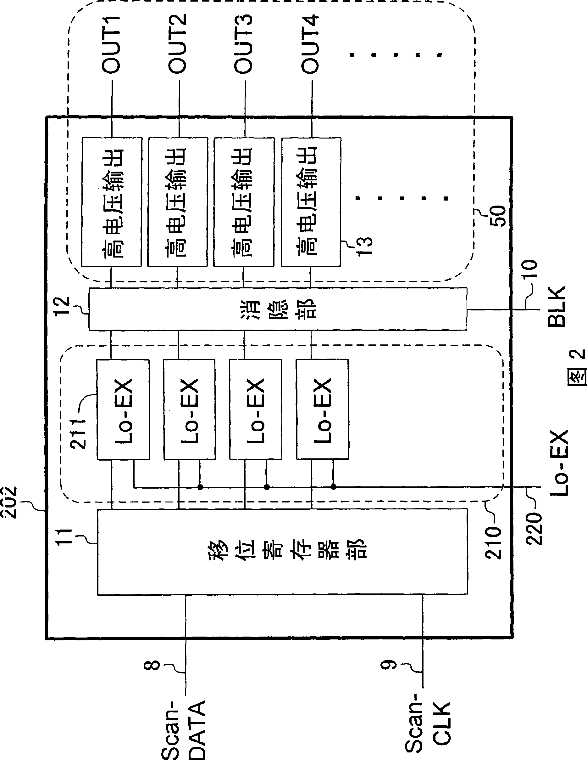
[0094] 6 is a block diagram showing the configuration of a scan drive unit (capacitive load drive circuit) according to a second embodiment of the present invention.
[0095] As shown in the figure, in the scan drive unit 350 of this embodiment, the high voltage output unit 13 of the scan drive unit 202 shown in FIG. Other configurations are the same as those of the scan drive unit 202 . The gain-variable high-voltage output block 300 is composed of a number of gain-variable high-voltage output units 301 corresponding to the scan electrodes. Each variable-gain high-voltage output unit 301 receives the output of the blanking unit 12 as an input, and supplies a signal to a corresponding scan electrode.
[0096] Next, a circuit configuration example and operation waveforms of the gain-variable high-voltage output unit 301 are shown using FIG. 7 . 7( a ) is a diagram showing a configuration example of the gain variable high voltage output unit 301 , and FIG. 7( b ) is a diagram ...
PUM
 Abstract
Description
Claims
Application Information
 - R&D Engineer
- R&D Manager
- IP Professional
- Industry Leading Data Capabilities
- Powerful AI technology
- Patent DNA Extraction
Browse by: Latest US Patents, China's latest patents, Technical Efficacy Thesaurus, Application Domain, Technology Topic, Popular Technical Reports.
© 2024 PatSnap. All rights reserved.Legal|Privacy policy|Modern Slavery Act Transparency Statement|Sitemap|About US| Contact US: help@patsnap.com