Driving method of liquid crystal display
A technology of a liquid crystal display and a driving method, which is applied in the field of driving of liquid crystal displays, can solve the problems of affecting display quality, display brightness distortion and the like
- Summary
- Abstract
- Description
- Claims
- Application Information
AI Technical Summary
Problems solved by technology
Method used
Image
Examples
no. 1 example
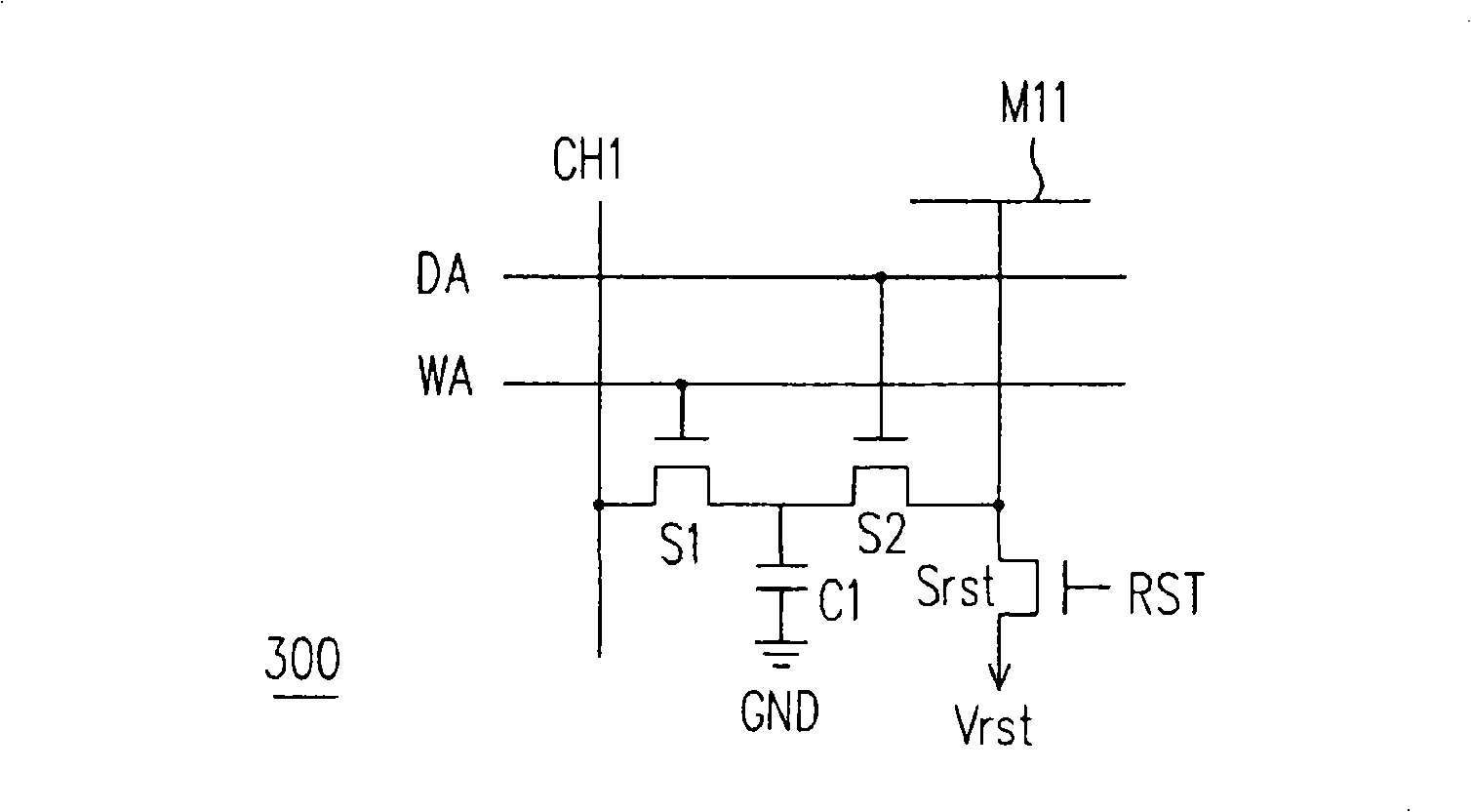
[0045] image 3 It is a driving circuit diagram of the liquid crystal unit in the first embodiment of the present invention. In this embodiment the switches are implemented as transistors, each transistor having a gate, a drain and a source. Please refer to image 3 , the liquid crystal unit 300 includes a first switch S1, a first capacitor C1, a second switch S2, a pixel electrode M11 and a reset switch Srst. The gate of the first switch S1 is coupled to the scan line WA, the source thereof is coupled to the data line CH1 , and the drain thereof is coupled to the first terminal of the first capacitor C1 . The second terminal of the first capacitor C1 is coupled to the ground terminal GND. The gate of the second switch S2 is coupled to the display signal line DA, the source thereof is coupled to the first terminal of the first capacitor C1 , and the drain thereof is coupled to the pixel electrode M11 . The reset switch Srst has its gate coupled to the reset signal line RST, ...
no. 2 example
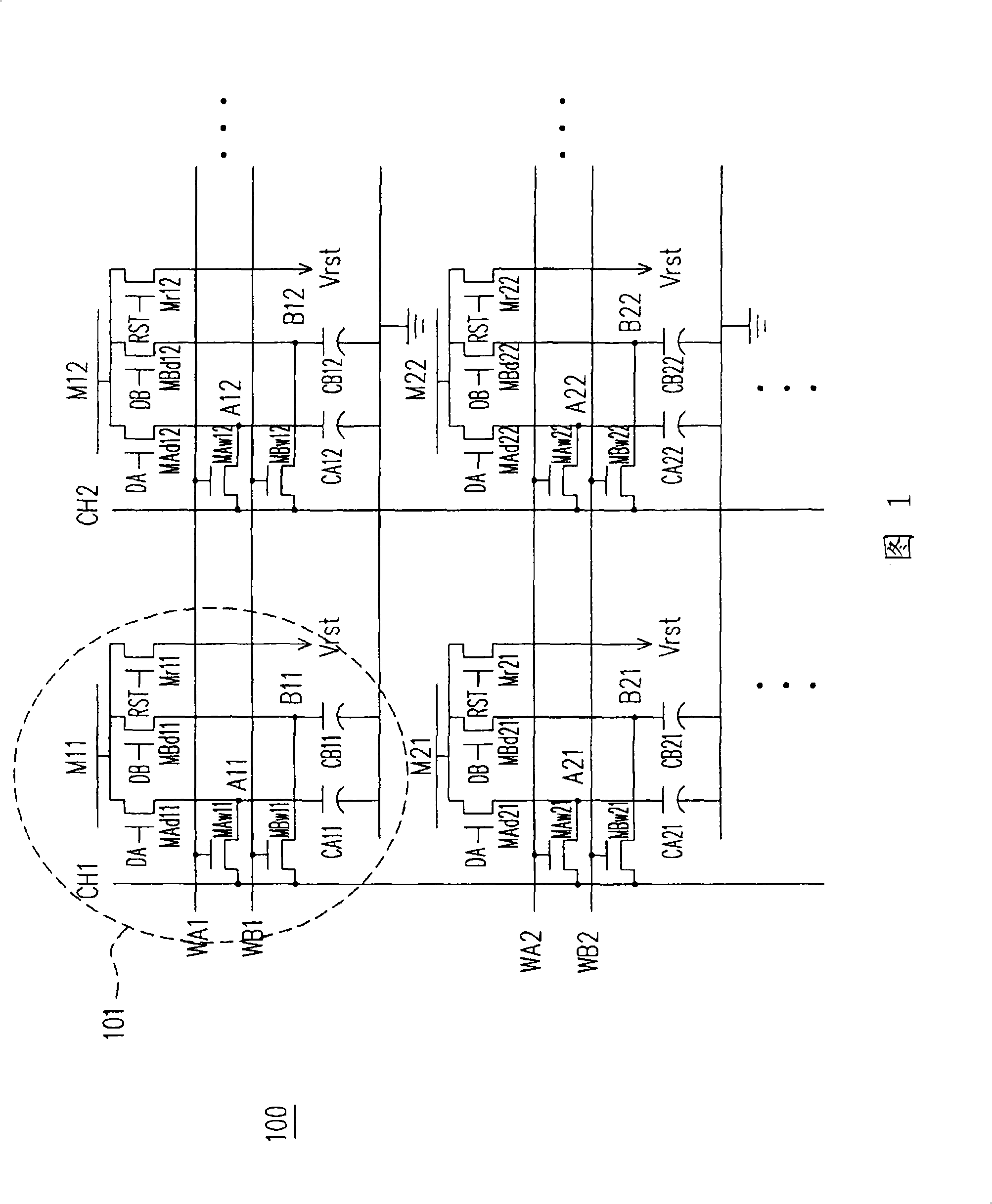
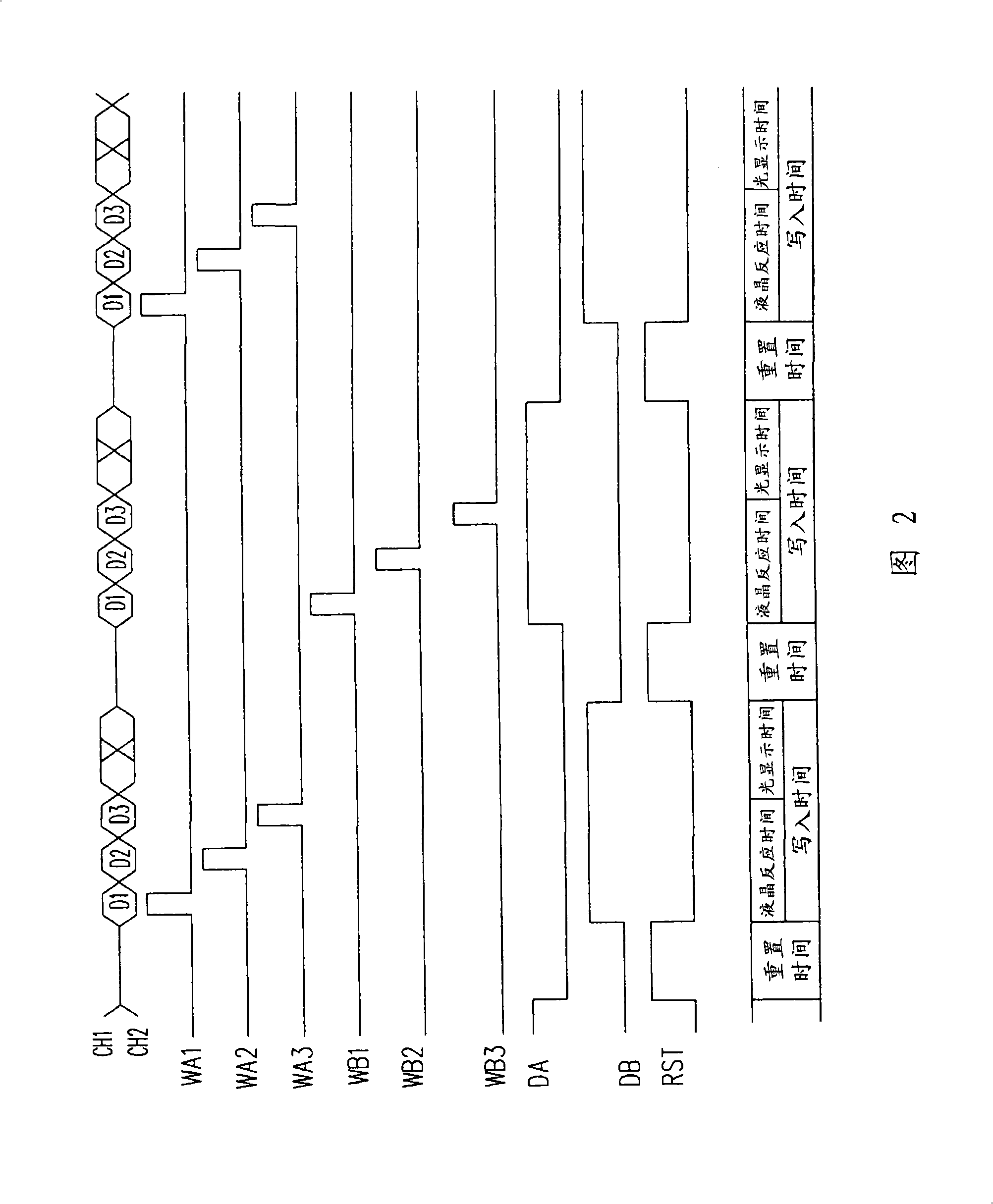
[0049] FIG. 5 is a driving circuit diagram of a liquid crystal display according to a second embodiment of the present invention. In this embodiment the switches are implemented as transistors, each transistor having a gate, a drain and a source. Please refer to FIG. 5 , the liquid crystal display 500 includes a plurality of liquid crystal cells. Taking the liquid crystal unit 501 as an example, it includes first and second writable switches TAw11 and TBw11, first and second storage capacitors CsA11 and CsB11, first and second displayable switches TAd11 and TBd11, pixel electrodes M11 and data Line CH1. Wherein, the liquid crystal display 500 displays the first and second frames during the first and second frame times, and each of the first and second frame times further includes liquid crystal response time, light display time and reset time.
[0050] The gate of the first writable switch TAw11 is coupled to the first scan line WA1 , the source thereof is coupled to the dat...
no. 3 example
[0056] FIG. 7 is a driving circuit diagram of a liquid crystal display according to a third embodiment of the present invention. In this embodiment the switches are implemented as transistors, each transistor having a gate, a drain and a source. Please refer to FIG. 7 , the liquid crystal display 700 includes a plurality of liquid crystal cells. Taking the liquid crystal unit 701 as an example, it includes first and second writable switches TAw11 and TBw11, first and second storage capacitors CsA11 and CsB11, first and second displayable switches TAd11 and TBd11, pixel electrodes M11, data Line CH1 and reset switch Tr11. Wherein, the liquid crystal display 700 displays the first and second frames during the first and second frame times, and each of the first and second frame times further includes liquid crystal response time, light display time and reset time.
[0057] The gate of the first writable switch TAw11 is coupled to the first scan line WA1 , the source thereof is ...
PUM
 Abstract
Description
Claims
Application Information
 - R&D Engineer
- R&D Manager
- IP Professional
- Industry Leading Data Capabilities
- Powerful AI technology
- Patent DNA Extraction
Browse by: Latest US Patents, China's latest patents, Technical Efficacy Thesaurus, Application Domain, Technology Topic, Popular Technical Reports.
© 2024 PatSnap. All rights reserved.Legal|Privacy policy|Modern Slavery Act Transparency Statement|Sitemap|About US| Contact US: help@patsnap.com


