Light source device and projector
一种光源装置、发光部的技术,应用在激光器装置、半导体激光器装置、放映装置等方向,能够解决隐患、介质流动停滞、显示品质降低等问题,达到抑制制造成本、易于控制、提高变换效率的效果
- Summary
- Abstract
- Description
- Claims
- Application Information
AI Technical Summary
Problems solved by technology
Method used
Image
Examples
no. 1 Embodiment approach
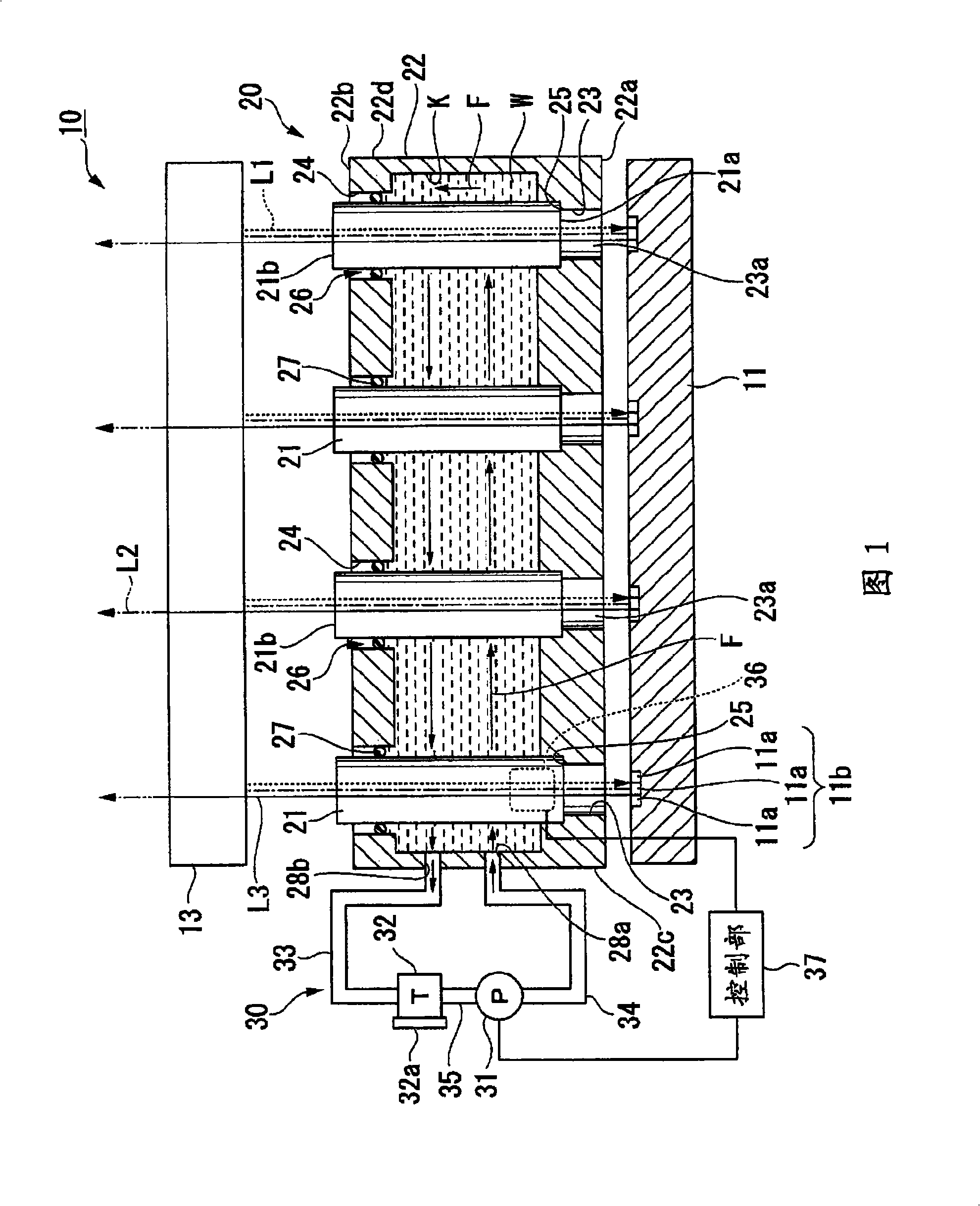
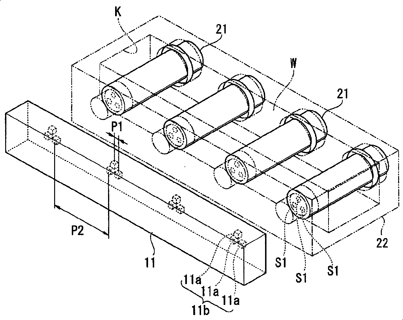
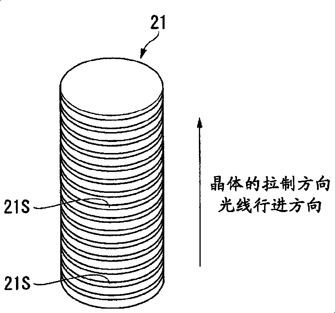
[0057] Refer to Figure 1 to image 3 A first embodiment of the present invention will be described.
[0058] FIG. 1 is a diagram showing a schematic configuration of a light source device, figure 2 It is a perspective view in which the wavelength selection element 13 of the light source device is omitted and the wavelength conversion element unit 20 is simplified, image 3 It is a perspective view of the wavelength conversion element. 1 shows only the optical path of the laser light emitted from one emitter for easy description of the optical path diagram of the light emitted from the semiconductor laser element to the wavelength selection element.
[0059] The light source device 10 of the present invention, as shown in FIG. The converted light and select the wavelength selective element 13 that reflects the light of the unconverted wavelength. In addition, the wavelength conversion element unit 20 includes four wavelength conversion elements 21 .
[0060] In the semicon...
no. 2 Embodiment approach
[0114] Next, a second embodiment of the present invention will be described with reference to FIG. 4 . In addition, in the drawings of the respective embodiments described below, the same reference numerals are attached to the same configuration as the light source device 10 of the first embodiment described above, and description thereof will be omitted.
[0115] In the light source device 40 of this embodiment, it differs from 1st Embodiment in the arrangement|positioning of the inlet 41a and the outlet 41b. Other configurations are the same as those of the first embodiment.
[0116] The inlet 41 a is provided on the left end surface 22 c of the holding member 22 , and the outlet 41 b is provided on the right end surface 22 d of the holding member 22 . That is, the inlet 41 a and the outlet 41 b face the housing space K of the holding member 22 and are formed in a direction parallel to the array direction of the wavelength conversion elements 21 (a direction perpendicular t...
no. 3 Embodiment approach
[0126] Next, a third embodiment of the present invention will be described with reference to FIG. 5 .
[0127] The light source device 50 of this embodiment is different from the first embodiment in that one wavelength conversion element 55 is used corresponding to one emitter 11 a. Other configurations are the same as those of the first embodiment.
[0128] In the semiconductor laser element 51, as shown in FIG. 5, eight emitters 51a are arranged in a row. In addition, the wavelength conversion element 55 is arranged to face each of the eight emitters 51a. Furthermore, the cross-sectional area of the wavelength conversion element 55 is such that a spot of light emitted from one emitter 51a can enter, and is smaller than the cross-sectional area of the wavelength conversion element 21 of the first embodiment. Thus, in the holding member 52 of the present embodiment, eight wavelength conversion elements 55 are used more than the holding member 22 of the first embodiment, ...
PUM
 Abstract
Description
Claims
Application Information
 - R&D
- Intellectual Property
- Life Sciences
- Materials
- Tech Scout
- Unparalleled Data Quality
- Higher Quality Content
- 60% Fewer Hallucinations
Browse by: Latest US Patents, China's latest patents, Technical Efficacy Thesaurus, Application Domain, Technology Topic, Popular Technical Reports.
© 2025 PatSnap. All rights reserved.Legal|Privacy policy|Modern Slavery Act Transparency Statement|Sitemap|About US| Contact US: help@patsnap.com


