
Device and method for real time observing colloid matter crystal internal defect

A technology of internal defects and colloidal crystals, applied in measuring devices, material analysis through optical means, instruments, etc., can solve problems such as blurred images, affecting the focus of microscopic imaging, and limiting the rotation range of imaging devices, so as to increase the magnification and Resolution, the effect of eliminating complicated steps

Inactive Publication Date: 2008-11-19
INST OF PHYSICS - CHINESE ACAD OF SCI
View PDF0 Cites 12 Cited by
  • Summary
  • Abstract
  • Description
  • Claims
  • Application Information

AI Technical Summary

Problems solved by technology

The larger the magnification of the microscope objective lens, the smaller the distance from the lens to the sample, which severely limits the rotation range of the imaging device, and also limits the magnification and spatial resolution of the imaging device.
In addition, the angle between the lens and the sample will affect the focus during microscopic imaging, resulting in blurred images

Method used


Image

  • Device and method for real time observing colloid matter crystal internal defect
  • Device and method for real time observing colloid matter crystal internal defect
  • Device and method for real time observing colloid matter crystal internal defect

Examples


Embodiment Construction

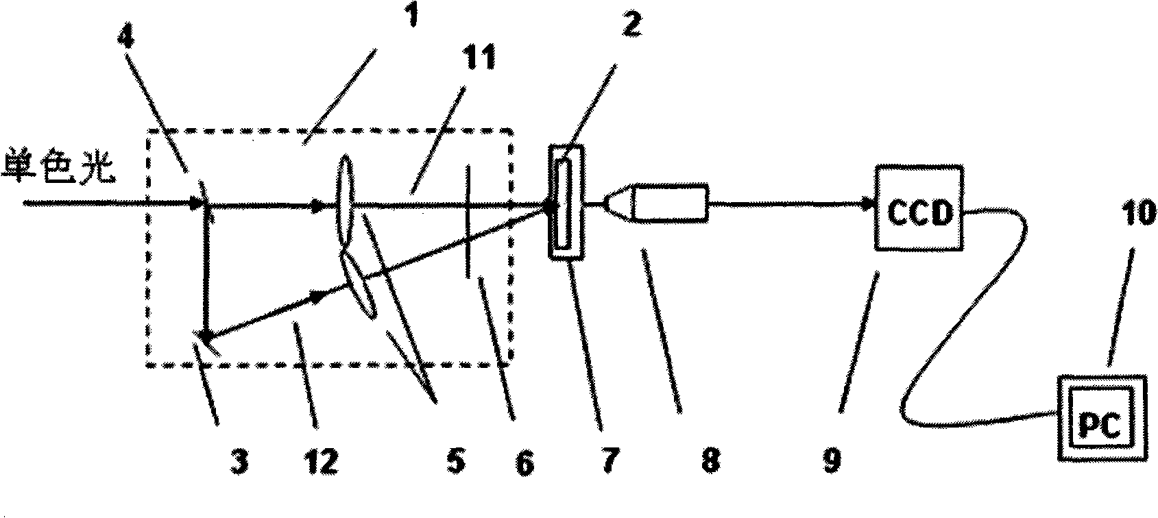
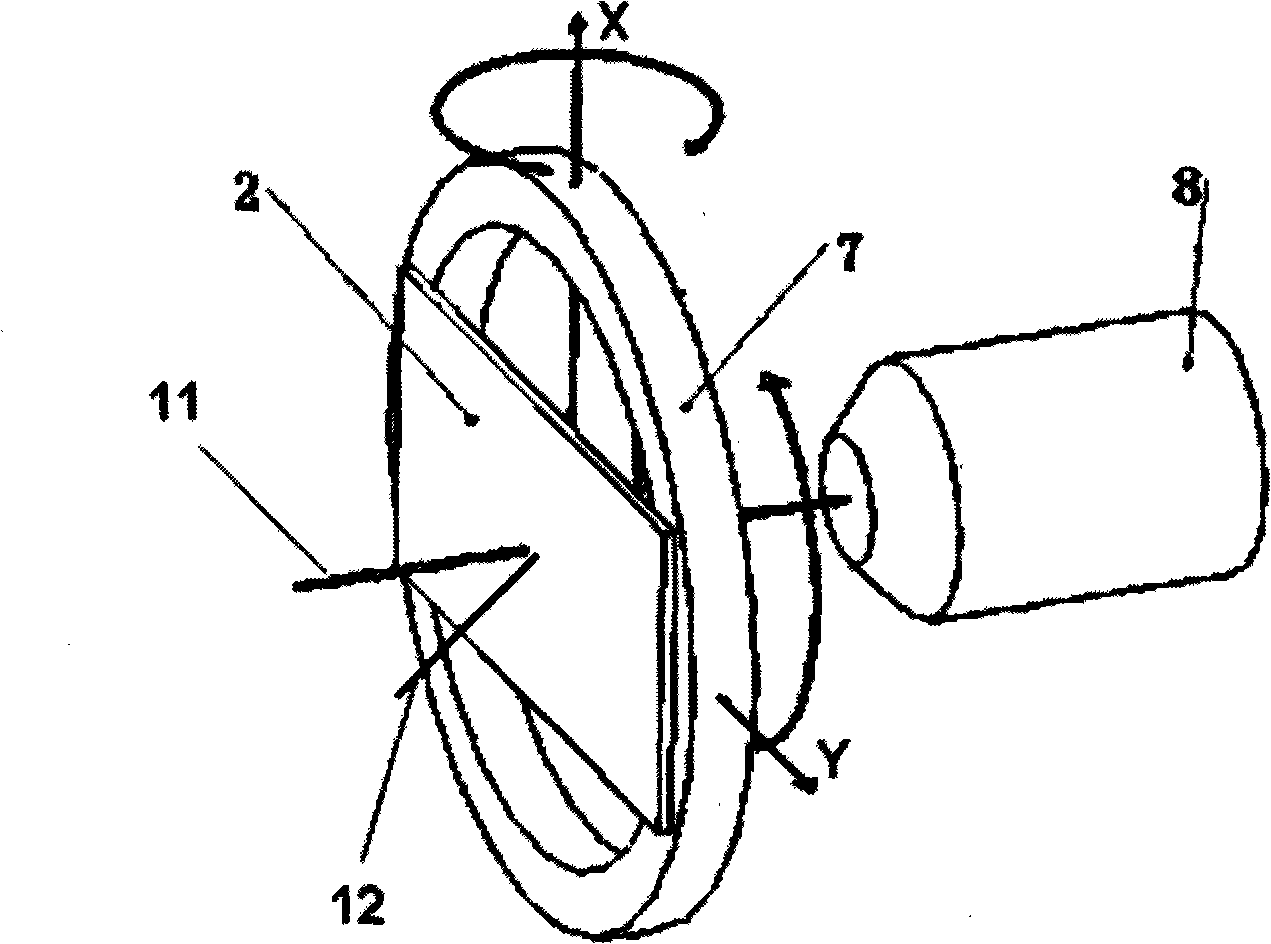
[0020] Such as figure 1 As shown, the device for real-time observation of internal defects of colloidal crystals in the present invention includes a light source, an illumination beam switching device 1, a sample 2 and a sample stage 7, a defect imaging device, and a central processing unit 10. The light source is a monochromatic light source; the illumination beam switching device 1 It includes a total reflection mirror 3, a half mirror 4, two focusing lenses 5 with long focal lengths, and a switcher 6. The switcher 6 is a baffle plate for selectively blocking the passage of incident light; the defect imaging device includes a microscope objective lens 8 and CCD (charge-coupled device) 9; the sample 2 is placed on the sample stage 7, and can move in a plane perpendicular to the optical axis, the illumination beam switching device 1 and the defect imaging device are respectively arranged on the front and the back of the sample 2, adjusting The distance between the microscope o...


PUM


Abstract

The invention discloses an apparatus for observing colloidal crystal internal defects in real time, which comprises: a light source, an illuminating beam change-over device, a sample stage, a defect imaging device and a central processing unit, and the illuminating beam change-over device, the sample stage and the defect imaging device are arrayed sequentially in tandem. The invention also discloses a method for observing colloidal crystal internal defects in real time, which concretely comprises the steps of: 1) irradiating a sample vertically by monochromatic light; 2) determining the direction of colloidal crystal diffracted light; 3) determining the direction of oblique incidence beams in the illuminating beam change-over device according to the direction of the diffracted light; 4) recording diffraction contrast images of colloidal crystal; and 5) image processing. The apparatus adopted in the invention can acquire bright and dark field images of diffraction contrast images of colloidal crystal internal defects, the bright or dark field images can be obtained without adjusting the crystal or moving the imaging device when observing the dark field images, a microscope objective is vertical to the surface of the sample all the time in the imaging process, thereby facilitating the usage of the objective with short working distance and high enlargement factor when in image formation.

Description

technical field [0001] The invention relates to a method and an imaging device for real-time observation of internal defects of colloidal crystals, belonging to the field of research on the structure and defects of colloidal crystals (including photonic crystals). Background technique [0002] Photonic crystals are photonic bandgap materials. From the perspective of material structure, photonic crystals are a kind of artificially designed and manufactured crystals with periodic dielectric structures on the wavelength scale of light. Similar to the modulation of electronic wave functions by semiconductor lattices, photonic bandgap materials can modulate electromagnetic waves with corresponding wavelengths---when electromagnetic waves propagate in photonic bandgap materials, they are modulated due to Bragg diffraction, and the energy of electromagnetic waves forms energy band structure. There is a band gap between the energy band and the energy band, that is, the photonic ba...

Claims


Application Information

Patent Timeline
IPC IPC(8): G01N21/958
Inventor 骆意勇吴兰生翟永亮李明
Owner INST OF PHYSICS - CHINESE ACAD OF SCI
Learn More