Array substrates of LCD devices

A technology of liquid crystal display devices and array substrates, which is applied in the directions of optics, instruments, and electrical components, and can solve problems such as data signal distortion, increased non-display area area, and large repair line resistance, so as to reduce resistance and data signal distortion , Improve the utilization rate, reduce the effect of resistance

Active Publication Date: 2010-06-02
KUSN INFOVISION OPTOELECTRONICS
View PDF2 Cites 0 Cited by
  • Summary
  • Abstract
  • Description
  • Claims
  • Application Information

AI Technical Summary

Problems solved by technology

For example, the array substrate needs to reserve a certain space in the non-display area to set the repair line, so the area of ​​the non-display area needs to be increased; in addition, when the above-mentioned repair line is used for repair, the resistance of the repair line itself is relatively large. distort the data signal

Method used


Image

  • Array substrates of LCD devices
  • Array substrates of LCD devices
  • Array substrates of LCD devices

Examples


Embodiment Construction

[0020] Exemplary embodiments of the present invention will be described in detail below with reference to the accompanying drawings. In addition, in this application, the orientation descriptions "upper", "lower", "left", "right", etc. are for the specific embodiments shown in the drawings, and may change according to specific implementation conditions .

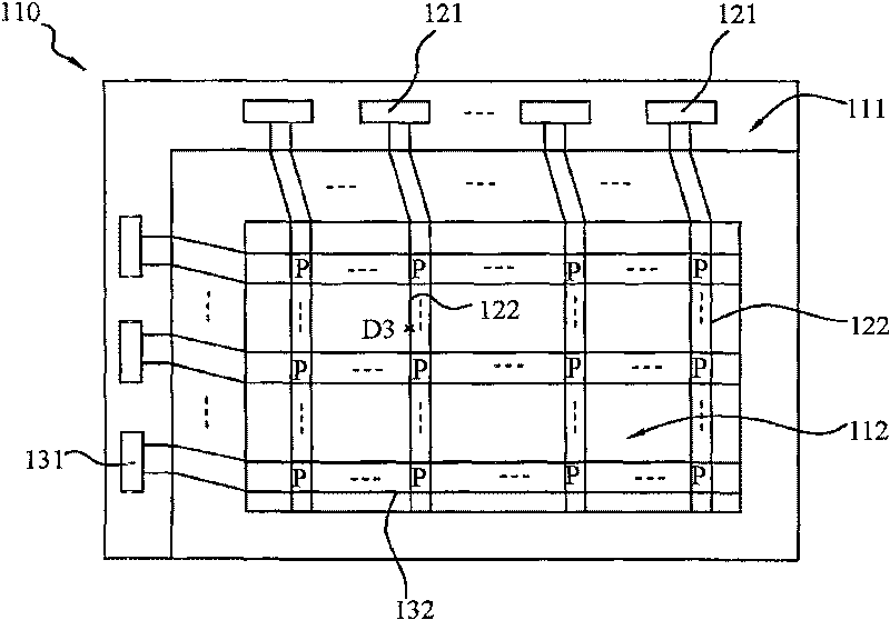
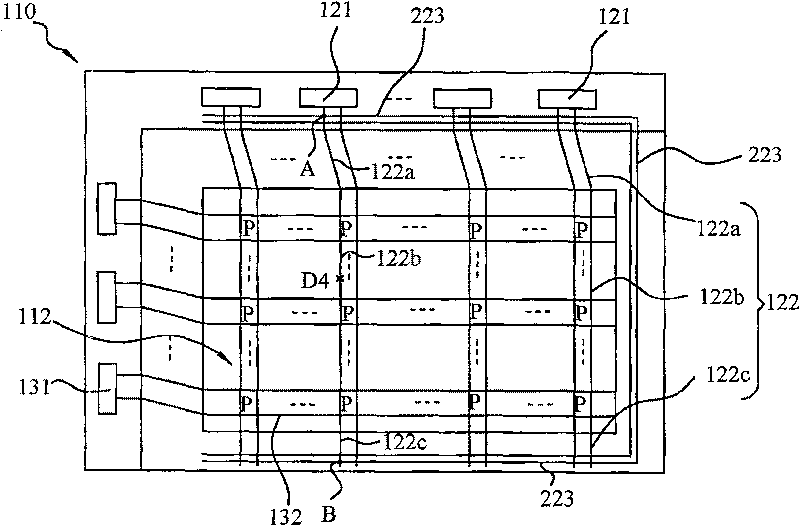
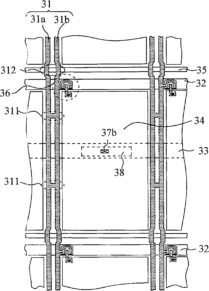
[0021] image 3 It is a partial plan view of the array substrate of the liquid crystal display device according to the first embodiment of the present invention, showing the repair circuit structure on the array substrate. The array substrate includes a plurality of data lines 31 and a plurality of scan lines 32 , and the data lines 31 and the scan lines 32 are vertically intersected to define a plurality of pixel regions. A pixel electrode 34 is formed in each pixel region, and a thin film transistor 36 is formed near the intersection of the data line 31 and the scan line 32 . The storage capacitor electrode 33 is arrang...


PUM


Abstract

The present invention provides an array substrate of a liquid crystal display device. The array substrate comprises a first scanning line, a second scanning line, a first data wire, a second data wire, and a pixel electrode. The first scanning line, the second scanning line, the first data wire and the second data wire are arranged crosswise and a pixel area in which the pixel electrode is provided is limited, wherein, the second data wire at least comprises a first branch and a second branch which are connected electrically. According to the invention, a space is not required to reserve for setting a mending wire. Therefore the area of non-display area is not required to enlarge and the usage factor of the array substrate is increased. As the shorter mending wire is used in the mending, the resistor of the mending wire and the distortion of data signal are reduced.

Description

technical field [0001] The invention relates to an array substrate of a liquid crystal display device, in particular to an array substrate of a liquid crystal display device with repaired lines. Background technique [0002] Liquid crystal display devices have the advantages of lightness, thinness, and low power consumption, so they are widely used in modern information equipment such as notebook computers, mobile phones, and personal digital assistants. [0003] figure 1 Shown is a schematic diagram of an array substrate in a conventional liquid crystal display device. The array substrate 110 of the liquid crystal display device includes a signal introduction region 111 and a display region 112 . Data line pads 121 and scan line pads 131 are formed in the signal introduction region 111 . The data lines 122 and the scan lines 132 are respectively connected to the data line pads 121 and the scan line pads 131 , and a plurality of pixels P are defined by intersection regions...

Claims


Application Information

Patent Timeline
Patent Type & Authority Patents(China)
IPC IPC(8): G02F1/1362G02F1/13H01L27/12
CPCG02F1/136259H01L27/1214H01L29/41733G02F2001/136272G02F2001/136263H01L27/12G02F1/136263G02F1/136272H01L27/124
Inventor 钟德镇简廷宪邱郁雯廖家德
Owner KUSN INFOVISION OPTOELECTRONICS
Why Eureka
Try Eureka