Method for measuring MOS transistor dismatching features

A technology of oxide semiconductors and measurement methods, applied in semiconductor/solid-state device testing/measurement, special data processing applications, instruments, etc., can solve problems such as inability to fully and truly reflect product mismatch characteristics

Inactive Publication Date: 2010-06-09
SEMICON MFG INT (SHANGHAI) CORP
View PDF7 Cites 0 Cited by
  • Summary
  • Abstract
  • Description
  • Claims
  • Application Information

AI Technical Summary

Problems solved by technology

However, the method of obtaining the mismatch characteristics of the same MOS transistor by computer simulation is realized based on building a model. The process of building a model is an approximate description of the real situation, and cannot fully and truly reflect the mismatch characteristics of the product.

Method used


Image

  • Method for measuring MOS transistor dismatching features
  • Method for measuring MOS transistor dismatching features
  • Method for measuring MOS transistor dismatching features

Examples


Embodiment Construction

[0044] The specific embodiments of the present invention will be described in detail below in conjunction with the accompanying drawings.

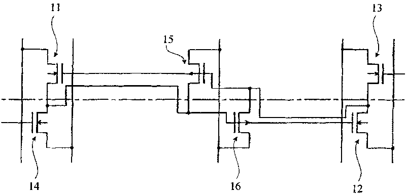
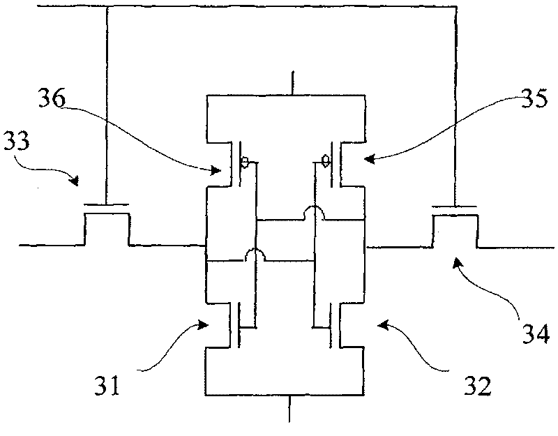
[0045]After a semiconductor device including two or more identical MOS transistors is manufactured, the matching degree of the two or more identical MOS transistors is often one of the main parameters for judging the performance of the semiconductor device. Since some semiconductor devices are sensitive to differences in electrical parameters of the same MOS transistors, that is, mismatch characteristics, it is necessary to understand such differences and minimize such differences. The invention provides a method for measuring the mismatch characteristic of a MOS transistor.

[0046] figure 2 It is a flow chart of an embodiment of the method for measuring mismatch characteristics of MOS transistors in the present invention.

[0047] Such as figure 2 In the flow chart shown, at first, at least one group of first layout patterns of semi...


PUM


Abstract

A method for measuring MOS transistor mismatch characteristic includes steps: generating at least one group of first edition patterns containing two or more same MOS transistors; generating at least one group of second edition patterns which have same pattern with the first edition pattern but have different arrangement angle with the first edition pattern; transferring the first edition patternsand the second edition patterns on a semiconductor chip and generating at least two groups of semiconductor devices having different arrangement angle on the semiconductor chip; measuring electric parameter of the MOS transistors in the semiconductor device; calculating difference of electric parameter for the MOS transistors having same structure and preparation technique in each group of semiconductor device; calculating standard deviation of the difference for the semiconductor devices having same arrangement angle and comparing the standard deviation of the semiconductor devices having different arrangement angle. The invention also provides a edition pattern and forming method thereof. The measuring method of present invention can truly and all sidedly reflect mismatch characteristicof same MOS transistor.

Description

technical field [0001] The invention relates to the technical field of semiconductor manufacturing and testing, in particular to a method for measuring mismatch characteristics of two or more identical metal oxide semiconductor transistors in a semiconductor device, a layout pattern and a forming method thereof. Background technique [0002] Metal-oxide-semiconductor transistors (Metal-Oxide-Semiconductor, MOS) have the advantages of low power consumption and fast response speed, and are widely used in the fields of computers, communications and storage. In some circuits using MOS transistors, two or more identical MOS transistors are often used. For example, a static random access memory (Static Random Access Memory, SRAM) storage unit. US Patent No. US 5744844 discloses a Static Random Access Memory (SRAM) storage unit composed of six MOS transistors. figure 1 It is a circuit diagram of the SRAM memory cell disclosed in the said US patent. Such as figure 1 As shown in ...

Claims


Application Information

Patent Timeline
Patent Type & Authority Patents(China)
IPC IPC(8): H01L21/66G06F17/50
Inventor 黄艳
Owner SEMICON MFG INT (SHANGHAI) CORP
Why Eureka
Try Eureka