
Method and apparatus for detecting unqualified silk screen printing mark

A technology of screen printing and marking, applied in measuring devices, instruments, etc., can solve the problems of inability to guarantee detection accuracy and low detection efficiency, and achieve the effect of saving time and energy, and improving efficiency and accuracy.

Inactive Publication Date: 2008-10-08
BEIJING XINWANG RUIJIE NETWORK TECH CO LTD
View PDF0 Cites 8 Cited by
  • Summary
  • Abstract
  • Description
  • Claims
  • Application Information

AI Technical Summary

Problems solved by technology

[0010] The invention provides a method and device for detecting unqualified silk screen marks, which are used to solve the problems in the prior art that the detection efficiency of unqualified silk screen marks is low and the detection accuracy cannot be guaranteed by manual methods

Method used


Image

  • Method and apparatus for detecting unqualified silk screen printing mark
  • Method and apparatus for detecting unqualified silk screen printing mark
  • Method and apparatus for detecting unqualified silk screen printing mark

Examples


Embodiment Construction

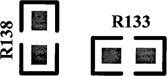
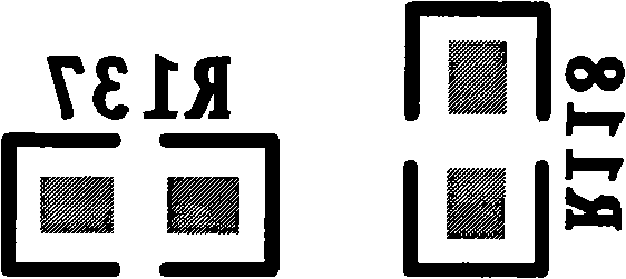
[0027] Embodiment 1 of the present invention provides a solution for detecting unqualified silk screen marks, which can automatically detect unqualified silk screen marks on the PCB, and solves the problems of low efficiency and low accuracy of manual detection in the prior art.

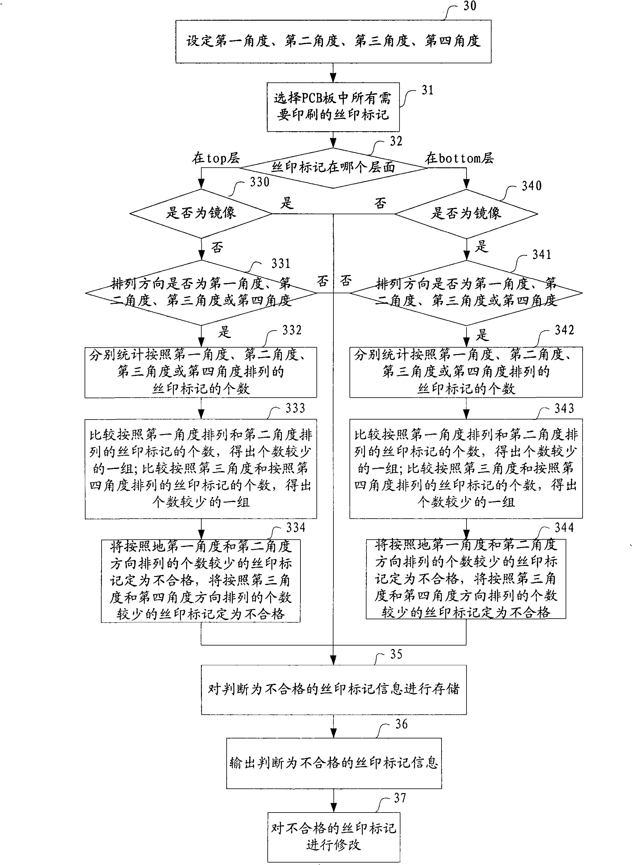
[0028] like image 3 As shown, it is a flow chart of a method for detecting unqualified silk screen marks provided by the present invention. The main implementation principles of the method are as follows:

[0029] Step 30, setting the first angle, the second angle, the third angle, and the fourth angle;

[0030] Wherein, the difference between the third angle and the first angle is 2n+1 (n is an integer) times of 90 degrees; the difference between the second angle and the first angle is 2n+1 (n is an integer) times of 180 degrees; the fourth The difference between the angle and the third angle is 2n+1 (n is an integer) times of 180 degrees. Preferably, for example, the first angle can be 0 degrees...


PUM


Abstract

The invemtion discloses a method for detecting an unqualified silkscreen, which comprises selecting the to-be detected silkscreen in the device selecting circuit board; and detecting the unqualified silkscreen with the layer arraying and the unqualified silkscreen with the angle arraying in the selected to-be detected silkscreen. The invention also discloses a detecting device corresponding to the detected unqualified silkscreen and the method and device for another detected unqualified silkscreen. The invention achieves the automated detection for the unqualified silkscreen, solving the problems of low efficiency of detecting the unqualified silkscreen manually and less assure for the precision.

Description

technical field [0001] The invention relates to the technical field of printed circuit board design, in particular to a method and device for detecting unqualified silk screen marks. Background technique [0002] In the design of printed circuit board (PCB, Print Circuit Board), the silk screen mark is the unique identification of the device. According to the silk screen mark, the actual position of the corresponding device can be found in the PCB board. Therefore, the mark is very important for the actual production of the PCB board. , debugging and maintenance play a very important auxiliary role. [0003] The information contained in the silk screen mark mainly includes device name information (REFDES), device pin number (pin number), description information placed on the surface, etc. The main function of this information is to indicate the approximate physical location of a component. In order to facilitate the production, debugging and maintenance of PCB boards. like...

Claims


Application Information

Patent Timeline
IPC IPC(8): G01B21/00
Inventor 王恩美
Owner BEIJING XINWANG RUIJIE NETWORK TECH CO LTD
Learn More