Display element and manufacturing and re-manufacturing method
A technology for display components and manufacturing methods, applied in nonlinear optics, instruments, optics, etc., can solve the problem that the scrap rate cannot be effectively reduced
- Summary
- Abstract
- Description
- Claims
- Application Information
AI Technical Summary
Problems solved by technology
Method used
Image
Examples
no. 1 example
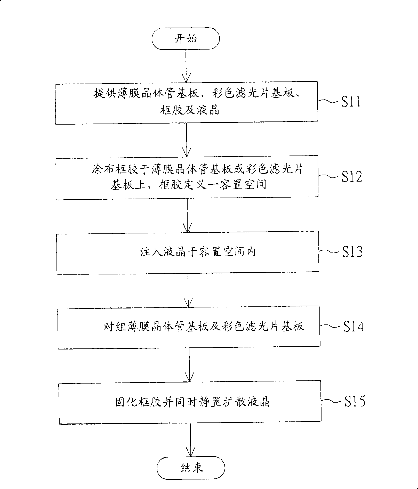
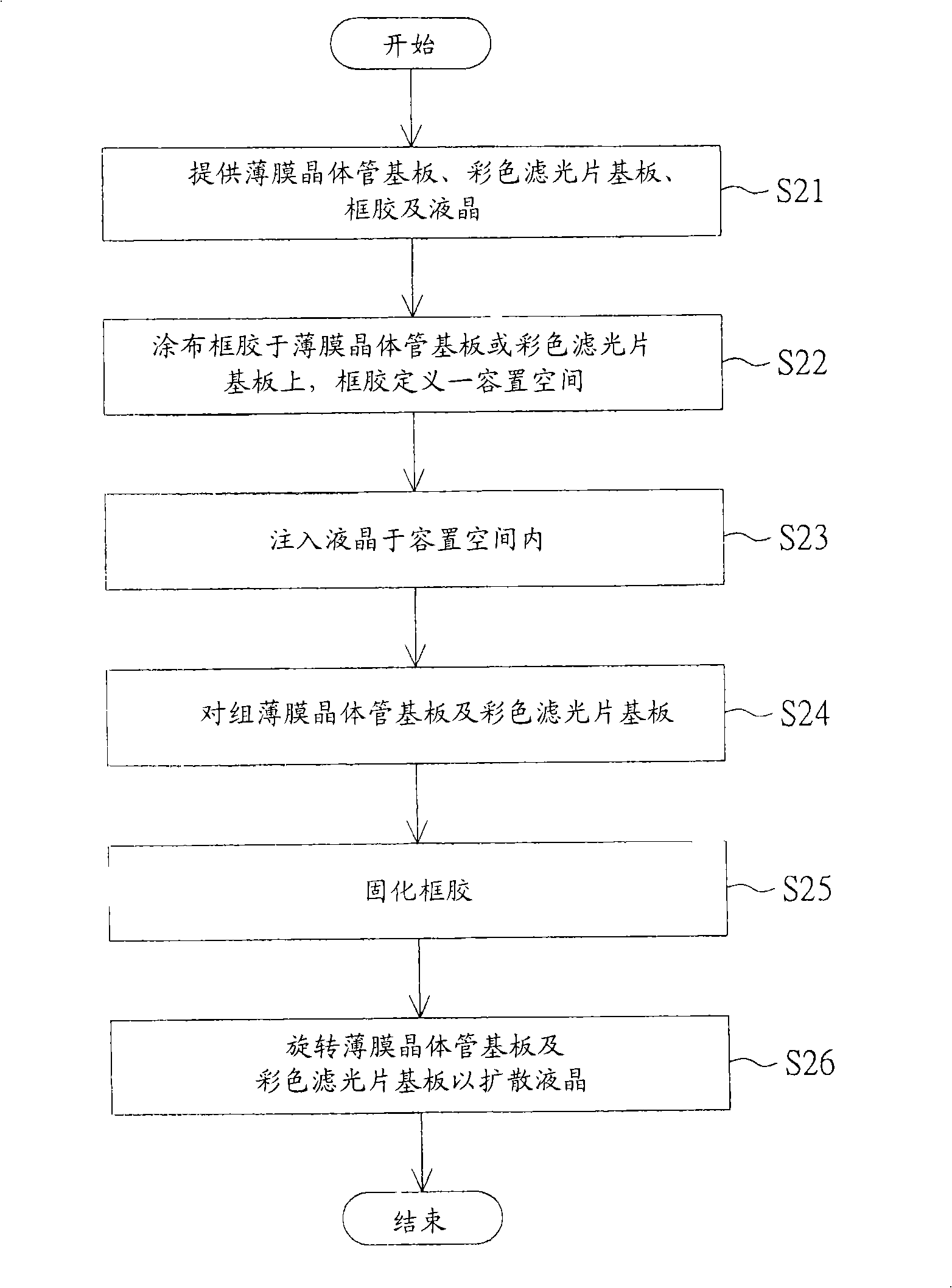
[0039] Please also refer to figure 2 and Figure 3A-3G , figure 2 A flowchart illustrating a method for manufacturing a display element according to a first embodiment of the present invention. Figure 3A-3G shown in accordance with figure 2 A schematic diagram of the steps. Such as Figure 3A As shown, the display element includes a thin-film transistor substrate (thin-film transistor substrate, TFT substrate) 11 , a color filter substrate (color filter substrate) 12 , frame glue 13 and liquid crystal 14 . The sealant 13 is disposed between the TFT substrate 11 and the color filter substrate 12 to form at least one accommodating space 15 . The liquid crystal 14 is injected into the accommodating space 15 and filled in the accommodating space 15 by a spinning process. First, in figure 2 In step S21, such as Figure 3A shown. A thin film transistor substrate 11 , a color filter substrate 12 , a sealant 13 and a liquid crystal 14 are provided.
[0040] Next, enter ...
no. 2 example
[0052] The liquid crystal diffusion method of the present invention can be applied to rework steps to shorten rework time. The display elements of this embodiment follow the reference numerals of the first embodiment, and will not be described again. Please refer to Figure 5A , which shows the inspection and rework flowchart of display components. During the manufacturing process of the display element, the liquid crystal 14 is diffused in the accommodating space 15 in various ways. However, the quality of the diffusion degree of the liquid crystal 14 greatly affects the quality of the display element, so the display element needs to undergo a testing process to ensure the quality. First, in step S501, a semi-finished display device is provided. Next, enter step S502 , turn on and detect whether the liquid crystal 14 of the display element completely covers the accommodating space 15 . If the liquid crystal 14 has filled the accommodating space 15 , the subsequent process...
no. 3 example
[0056] The difference between the manufacturing method of the display element of this embodiment and the manufacturing method of the display element of the first embodiment lies in the way of liquid crystal injection, and the rest of the same parts will not be repeated. Please also refer to Figure 7 and Figures 8A-8G , Figure 7 A flowchart illustrating a manufacturing method of a display element according to a third embodiment of the present invention. Figures 8A-8G shown in accordance with Figure 7 A schematic diagram of the steps. First, in Figure 7 In step S71, such as Figure 8A shown. A thin film transistor substrate 11 , a color filter substrate 12 and a sealant 13 are provided.
[0057] Next, enter Figure 7 Step S72 , coating the sealant 13 on the TFT substrate 11 or the color filter substrate 12 . Such as Figure 8A As shown, sealant 13 is coated on the color filter substrate 12 to form four accommodating spaces 15 . Wherein, the sealant 13 has a gap ...
PUM
 Abstract
Description
Claims
Application Information
 - R&D Engineer
- R&D Manager
- IP Professional
- Industry Leading Data Capabilities
- Powerful AI technology
- Patent DNA Extraction
Browse by: Latest US Patents, China's latest patents, Technical Efficacy Thesaurus, Application Domain, Technology Topic, Popular Technical Reports.
© 2024 PatSnap. All rights reserved.Legal|Privacy policy|Modern Slavery Act Transparency Statement|Sitemap|About US| Contact US: help@patsnap.com


