
High pass filter circuit with low corner frequency

A high-pass filter circuit and frequency reduction technology, which can be applied to logic circuits with logic functions, frequency selection two-terminal pair networks, electrical components, etc., and can solve problems such as cost increase

Inactive Publication Date: 2008-08-13
MEDIATEK INC
View PDF1 Cites 8 Cited by
  • Summary
  • Abstract
  • Description
  • Claims
  • Application Information

AI Technical Summary

Problems solved by technology

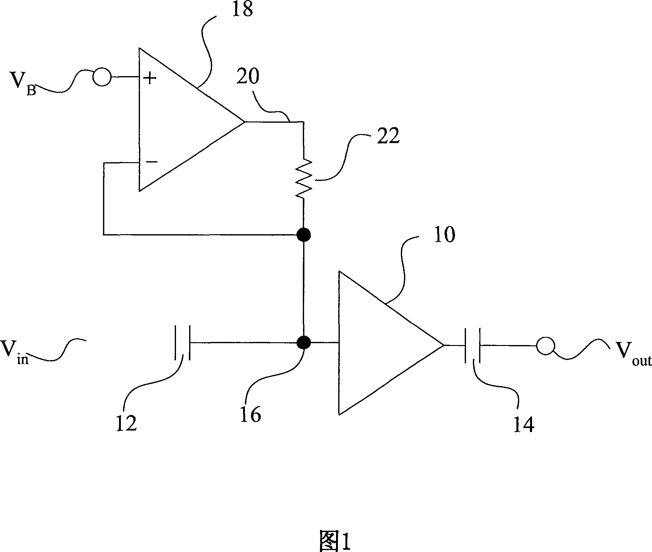
However, the resistor 22 having a large impedance occupies a large area in the integrated circuit, which represents an increase in cost

Method used


Image

  • High pass filter circuit with low corner frequency
  • High pass filter circuit with low corner frequency
  • High pass filter circuit with low corner frequency

Examples


Embodiment Construction

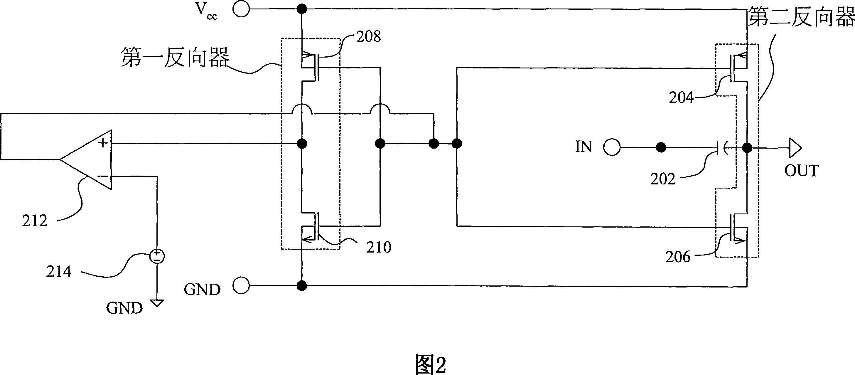
[0024] Please refer to FIG. 2 , which is a circuit diagram of a high-pass filter circuit using CMOS to provide a large resistance according to a preferred embodiment of the present invention. The high-pass filter circuit has a signal input terminal IN and a signal output terminal OUT, and has a capacitor 202, a first inverter composed of transistors 208, 210 and a second inverter composed of transistors 204, 206, A voltage source 214 and an operational amplifier 212 . To eliminate the DC offset, the capacitor 202 is coupled to the second inverter providing a large impedance to generate an AC-coupling to eliminate the DC offset. In the first and second inverters of the preferred embodiment of the present invention, the aforementioned transistors are CMOS transistors. The transistors 204 and 208 are p-CMOS transistors, and the transistors 206 and 210 are n-CMOS transistors. The capacitor 202 is coupled between the signal input terminal IN and the signal output terminal OUT. T...


PUM


Abstract

A high pass filter circuit having a signal input terminal and a signal output terminal. The high pass filter circuit is provided with a voltage source, first and second inverters, and a capacitor. The voltage source provides a DC bias voltage. The first inverter couples to the voltage source to invert the DC bias voltage. The second inverter couples to the first inverter and a signal output terminal respectively. The second inverter inverts the DC bias voltage inverted by the first inverter to provide the DC bias voltage to the signal output terminal. The second inverter also provides large impedance at the signal output terminal. The capacitor is coupled between the signal input terminal and the signal output terminal to provide a low corner frequency in cooperation with the second inverter. The circuit further comprises an operational amplifier. The voltage source provides the DC bias voltage through the operational amplifier to avoid the total impedance at the output terminal that is decreased by the voltage source.

Description

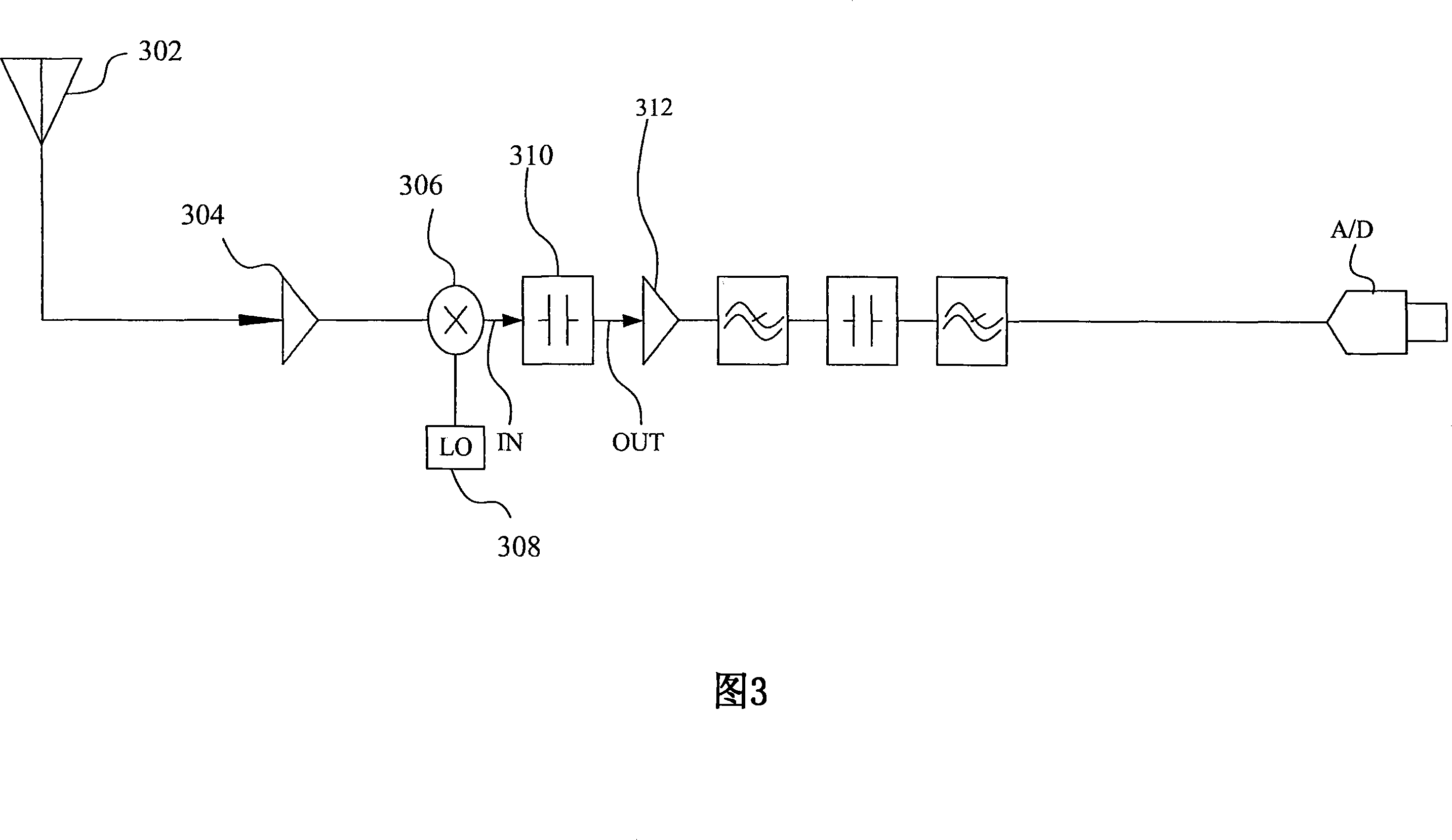
technical field [0001] The present invention relates to a high-pass filter circuit, in particular to a high-pass filter circuit with low corner frequency and providing precise bias voltage. Background technique [0002] The technology of direct frequency reduction has been widely used in radio frequency (RF) applications today. For a direct conversion receiver (DCR), the elimination of the DC voltage deviation is a very important issue. For example, an AC coupling circuit is used to eliminate the deviation of the DC voltage to filter the deviation and allow the desired signal to pass through the circuit for subsequent signal processing. In addition, a DC bias voltage must also be provided for subsequent signal processing modules, such as an analog-to-digital converter (ADC). [0003] For example, FIG. 1 shows a non-inductive voltage bias circuit disclosed in US Pat. No. 5,760,651 in the prior art. Amplifiers 10 are respectively coupled at the input terminals V in and the...

Claims


Application Information

Patent Timeline
Patent Type & Authority Applications(China)
IPC IPC(8): H03H11/04H03F1/30H03F3/45H03K19/20H03D7/00
CPCH03H11/04
Inventor 屈庆勋崔吉青
Owner MEDIATEK INC
Learn More