Semiconductor device, method of manufacturing semiconductor device, and electronic apparatus
A manufacturing method and semiconductor technology, which is applied in semiconductor/solid-state device manufacturing, semiconductor devices, semiconductor/solid-state device components, etc., can solve problems such as poor operation of semiconductor devices, and achieve the effects of increased strength, high reliability, and prevention of breakage
- Summary
- Abstract
- Description
- Claims
- Application Information
AI Technical Summary
Problems solved by technology
Method used
Image

Examples
no. 1 Embodiment approach
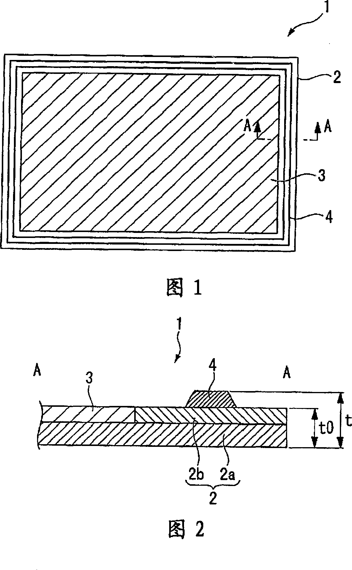
[0054] A first embodiment of the present invention will be described. FIG. 1 is a plan view showing the structure of a semiconductor device according to this embodiment.
[0055] As shown in the figure, a semiconductor device 1 is mainly composed of a substrate 2 , a thin film circuit layer 3 , and a reinforcing part 4 . The thin film circuit layer 3 is provided at the center of the substrate 2 as viewed in plan, and is a circuit including semiconductor elements and the like. The reinforcement part 4 is provided on the substrate 2 so as to surround the thin film circuit layer 3, and is a rib part made of resin such as acrylic or polyimide, for example.
[0056] Fig. 2 is a diagram showing the structure along the A-A section in Fig. 1 .
[0057] As shown in FIG. 2, the substrate 2 is mainly composed of a base material 2a and a surface layer 2b, and has a structure in which the surface layer 2b is laminated on the base material 2a. The substrate 2a is made of a resin material, ...
no. 2 Embodiment approach
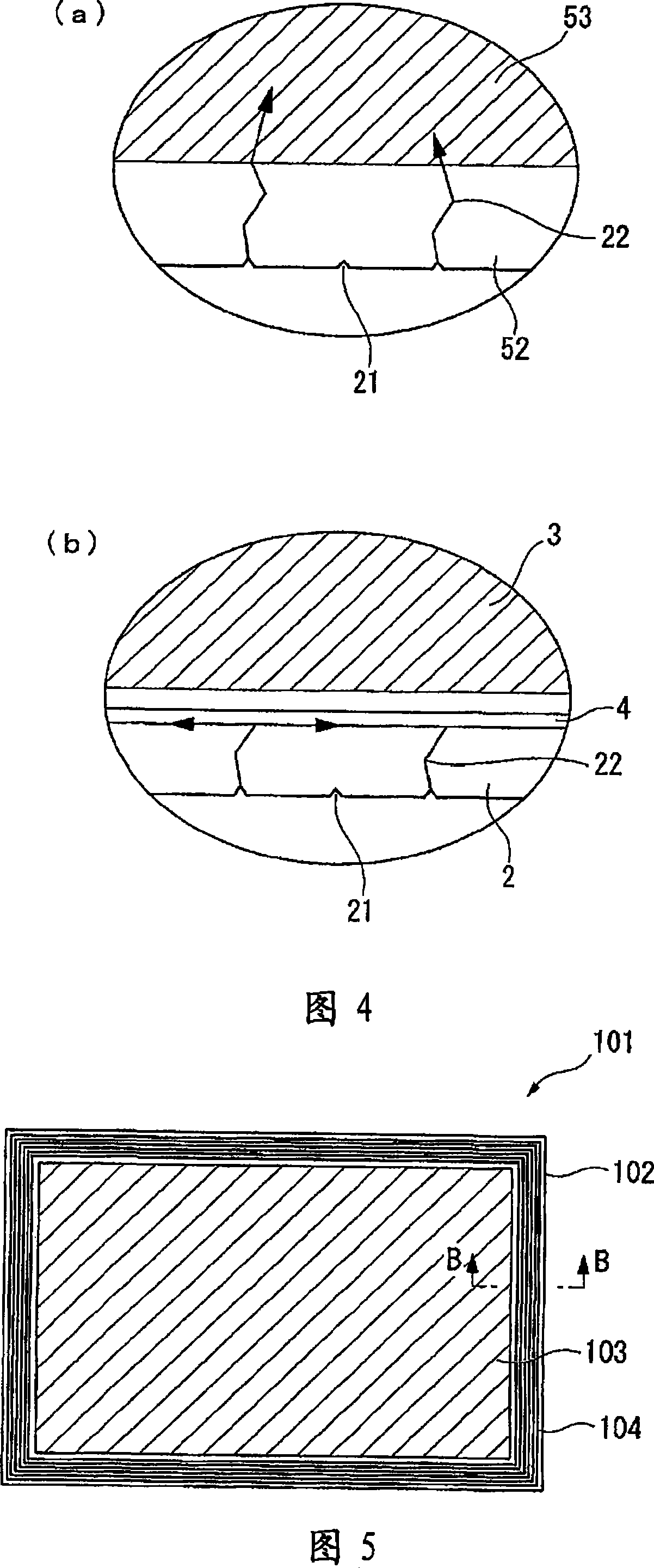
[0065] Next, a second embodiment of the present invention will be described. FIG. 5 is a plan view showing the structure of the semiconductor device of the present embodiment. FIG. 6 is a cross-sectional view showing the structure along the B-B cross-section in FIG. 5 .
[0066] As shown in FIG. 5 , the semiconductor device 101 is mainly composed of a substrate 102 , a thin film circuit layer 103 , and a reinforcing part 104 . Like the first embodiment, the thin film circuit layer 103 is provided at the center of the substrate 102 in plan view. In the present embodiment, the reinforcement part 104 has a structure in which multiple layers are provided on the substrate 102 so as to surround the thin film circuit layer 103. In FIGS. 5 and 6, for example, the rib part is provided triple.
[0067] As described above, according to the present embodiment, since the ridges constituting the reinforcing portion 104 are provided multiple times, it is possible to multiplex protect crack...
no. 3 Embodiment approach
[0069] Next, a third embodiment of the present invention will be described. FIG. 7 is a plan view showing the configuration of a liquid crystal device 201 of the present embodiment.
[0070] As shown in the figure, the liquid crystal device 201 has a structure in which, for example, a TFT array substrate 210 made of a transparent resin material such as acrylic or PES and a counter substrate 220 are stacked and a sealing material (not shown) is provided between them. shown) to make it bonded. A liquid crystal layer (not shown) is sealed in the region surrounded by the sealing material. A region inside the sealing material becomes a light modulation region 203 that modulates light from the outside.
[0071] In the TFT array substrate 210, in the region (protruding region) protruding from the opposite substrate 220, driving circuits such as the scanning line driving circuit 205 and the data line driving circuit 206 are formed. The inter-substrate conducting portion 207 for ach...
PUM
 Abstract
Description
Claims
Application Information
 - Generate Ideas
- Intellectual Property
- Life Sciences
- Materials
- Tech Scout
- Unparalleled Data Quality
- Higher Quality Content
- 60% Fewer Hallucinations
Browse by: Latest US Patents, China's latest patents, Technical Efficacy Thesaurus, Application Domain, Technology Topic, Popular Technical Reports.
© 2025 PatSnap. All rights reserved.Legal|Privacy policy|Modern Slavery Act Transparency Statement|Sitemap|About US| Contact US: help@patsnap.com