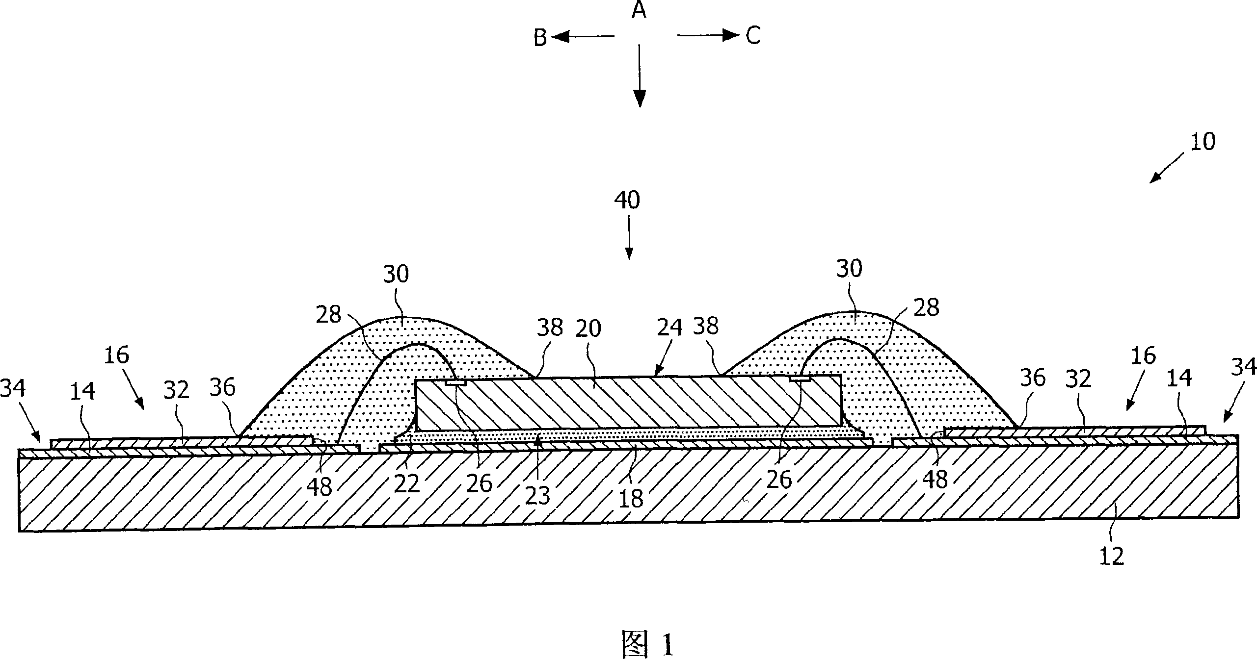
A package and manufacturing method for a microelectronic component
A technology of microelectronics and components, applied in the field of packaging of microelectronic components, can solve the problems of bonding pad pollution, easy damage of microelectronic devices, etc.
- Summary
- Abstract
- Description
- Claims
- Application Information
AI Technical Summary
Problems solved by technology
Method used
Image
Examples
Embodiment Construction
[0033] In Fig. 3, a cross-sectional view of package 70 is shown, taken along line 3-3 in Fig. 4b. The package 70 includes a dam 44 provided on the outer layer 32 on the first side. The dam comprises a stepped surface transition 46 between the outer layer 32 and the wire 14 or a layer 49 below the outer layer (see FIGS. 4a and 4b ). During the curing of the glob material 30 , the dam affects the shape of the glob material 30 to expand the width L of the central region 40 and thus the surface area of the central region. Each inner edge 48 of the outer layer 32 (see FIG. 1 ) is processed, the sealing material is faced in place and an additional layer is applied on top of the layer 32 parallel to said edge of the layer 32, thereby forming a dam 44, as shown in Figure 3. Another solution is to arrange the edge 48 of the outer layer 32 closer to the outside of the carrier element 12, and an additional layer is applied on top of the conductive tracks and the first bottom layer, t...
PUM
 Abstract
Description
Claims
Application Information
 - R&D
- Intellectual Property
- Life Sciences
- Materials
- Tech Scout
- Unparalleled Data Quality
- Higher Quality Content
- 60% Fewer Hallucinations
Browse by: Latest US Patents, China's latest patents, Technical Efficacy Thesaurus, Application Domain, Technology Topic, Popular Technical Reports.
© 2025 PatSnap. All rights reserved.Legal|Privacy policy|Modern Slavery Act Transparency Statement|Sitemap|About US| Contact US: help@patsnap.com


