Metal gate mosfet by full semiconductor metal alloy conversion

一种金属合金、半导体的技术,应用在MOSFET器件的结构领域,能够解决很难集成nFET和pFET器件等问题

Inactive Publication Date: 2008-07-30
INT BUSINESS MASCH CORP
View PDF0 Cites 2 Cited by
  • Summary
  • Abstract
  • Description
  • Claims
  • Application Information

AI Technical Summary

Problems solved by technology

Using different processes for silicidation of nFET and pFET gate conductors makes it difficult to integrate both nFET and pFET devices, especially in densely packed memory cells

Method used


Image

  • Metal gate mosfet by full semiconductor metal alloy conversion
  • Metal gate mosfet by full semiconductor metal alloy conversion
  • Metal gate mosfet by full semiconductor metal alloy conversion

Examples


Embodiment Construction

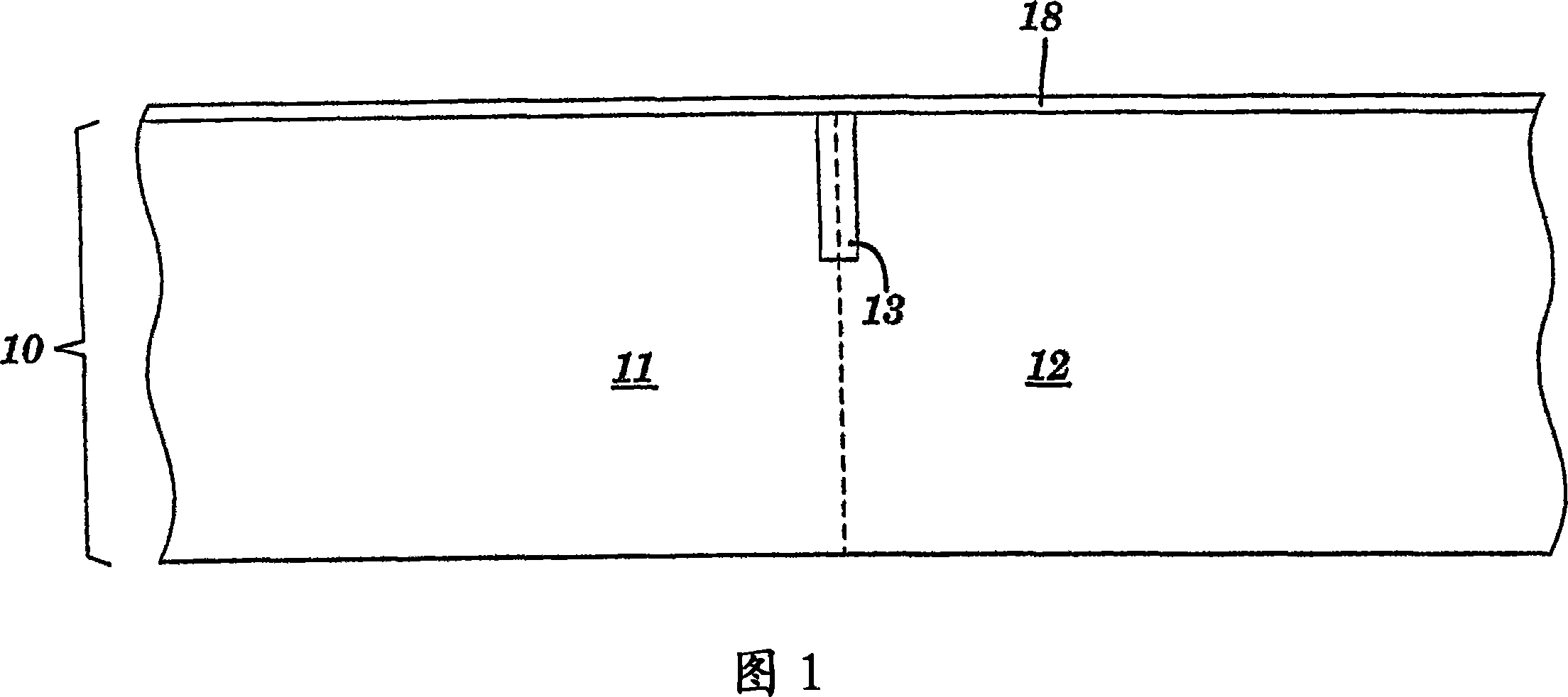
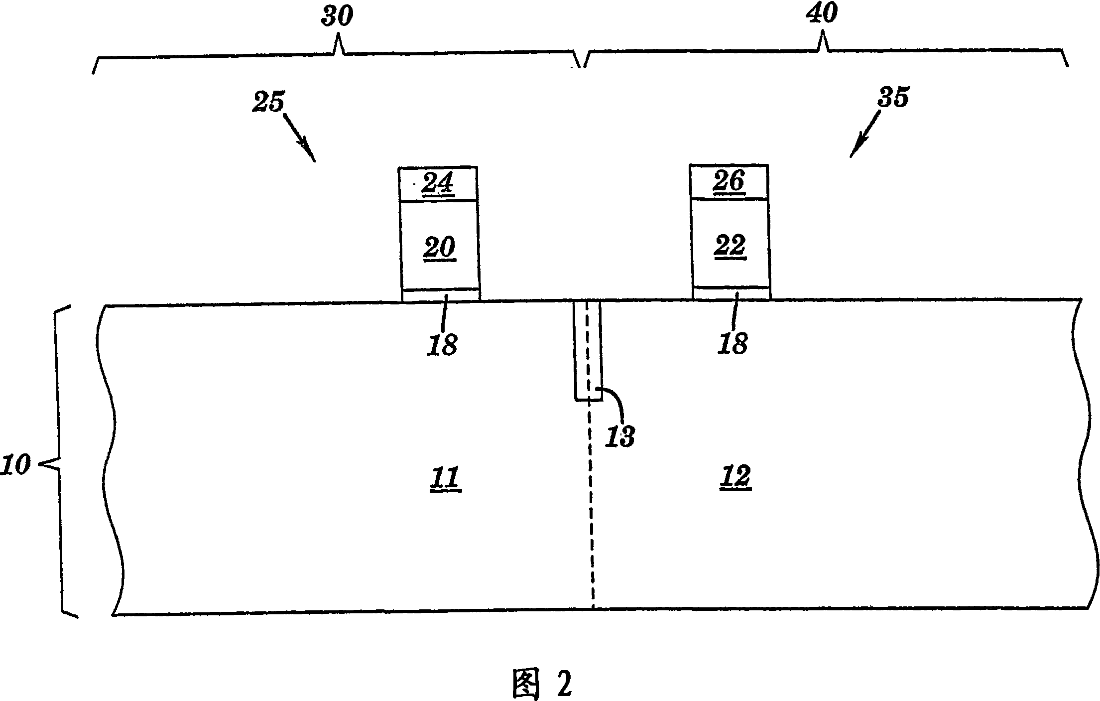
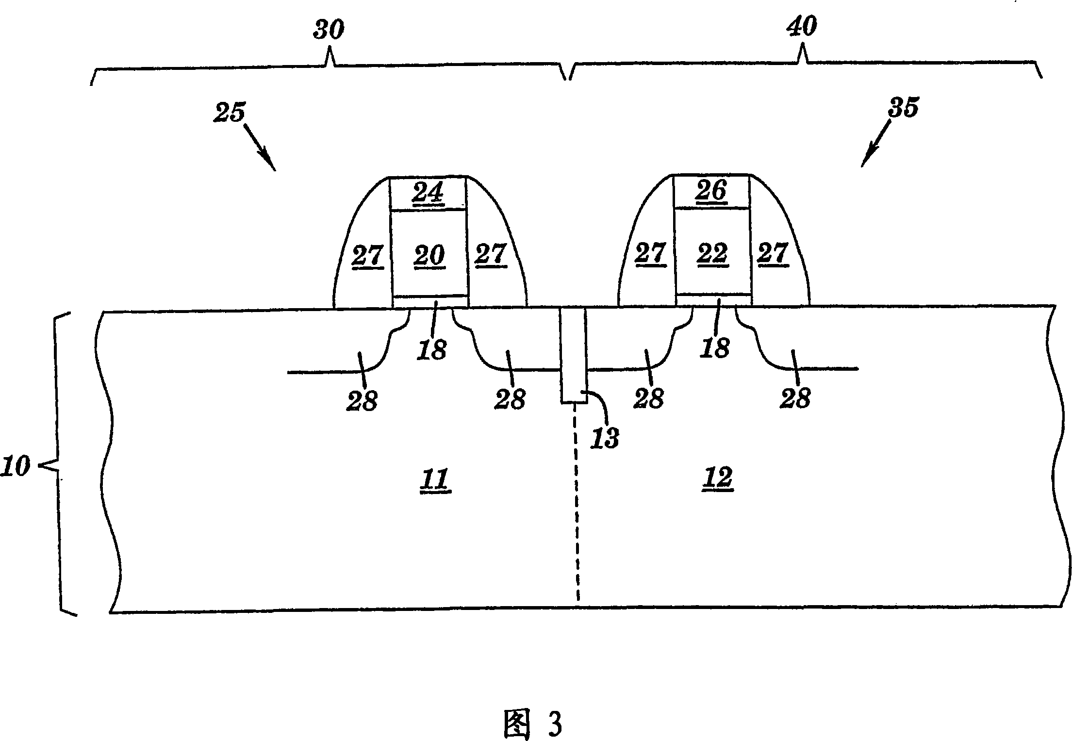
[0017] The present invention will now be described in detail with reference to the drawings accompanying this application, in which the present invention provides a method for combining a MOSFET device of a first type (e.g., nFET) having a fully silicided gate electrode with a MOSFET device having a partially silicided gate electrode. Structures and methods for integrating MOSFET devices of a second type (eg, pFET).

[0018] In accordance with the present invention, a process flow is provided wherein a first type of MOSFET device includes a fully silicided gate electrode, and a second type of MOSFET device has a partially silicided electrode such that both devices have a similar standard polysilicon gate electrode approach. threshold voltage. The techniques described in this disclosure can be applied to densely packed circuits with gate gaps of less than about 200 nm. In the exemplary embodiments described hereinafter, nFETs are implemented with fully silicided gate electrode...


PUM


Abstract

A MOSFET structure and method of forming is described. The method includes forming a metal-containing layer (56) that is thick enough to fully convert the semiconductor layer (22) to a semiconductor metal alloy in a first MOSFET type region (40) but only thick enough to partially convert the semiconductor layer (20) to a semiconductor metal alloy in a second MOSFET type region (30). In one embodiment, the gate stack in a first MOSFET region (40) is recessed prior to forming the metal-containing layer (56) so that the height of the first MOSFET semiconductor stack is less than the height of the second MOSFET semiconductor stack. In another embodiment, the metal-containing layer (56) is thinned over a first type MOSFET region (40) relative to a second type MOSFET region (30) prior to the conversion process.

Description

technical field [0001] The present invention relates generally to the fabrication of integrated circuits, and more particularly to structures and methods of fabricating MOSFET (Metal Oxide Semiconductor Field Effect Transistor) devices having metal gates. Background technique [0002] Metal gate technology allows for improved MOSFET device performance compared to conventional semiconductor MOSFET devices using semiconductor gate electrodes due to the elimination of the depletion layer in the gate; thus, converting the electrical transition oxide thickness t inv A decrease of about 3-5 Å without resulting in a significant increase in gate oxide leakage current followed. Typically, the semiconductor gate electrode is formed of polysilicon (poly or poly-Si, amorphous silicon, SiGe, etc.). MOSFET devices with a fully silicided gate electrode (FUSI gate) allow for a thinner electrical transition oxide thickness t inv , which lead to improved device performance due to increased ...

Claims


Application Information

Patent Timeline
Patent Type & Authority Applications(China)
IPC IPC(8): H01L21/8238H01L21/336H01L21/8234H01L21/4763H01L29/00
CPCH01L29/66545H01L29/7833H01L21/823842H01L29/6659H01L21/823835H01L21/18H01L21/8238H01L29/00
Inventor H·M·内伊费M·库玛尔方隼飞J·T·凯德齐尔斯基C·小卡布拉尔
Owner INT BUSINESS MASCH CORP
Why Eureka
Try Eureka