
Adapter of transmission electron microscope example bench, its substrate and manufacturing method thereof

A technology of electron microscope and adapter, applied in the direction of circuits, discharge tubes, electrical components, etc., can solve problems such as inability to measure material properties

Active Publication Date: 2008-07-16
INST OF PHYSICS - CHINESE ACAD OF SCI
View PDF0 Cites 16 Cited by
  • Summary
  • Abstract
  • Description
  • Claims
  • Application Information

AI Technical Summary

Problems solved by technology

[0003] The purpose of the present invention is to solve the technical problem that the current transmission electron microscope (TEM) sample stage cannot measure the properties of materials, so as to realize the research of materials, especially nanometer materials. The purpose of the relationship between the microstructure and properties of the same tiny region

Method used


Image

  • Adapter of transmission electron microscope example bench, its substrate and manufacturing method thereof
  • Adapter of transmission electron microscope example bench, its substrate and manufacturing method thereof
  • Adapter of transmission electron microscope example bench, its substrate and manufacturing method thereof

Examples


Embodiment Construction

[0028] Below in conjunction with accompanying drawing, the present invention is described in further detail:

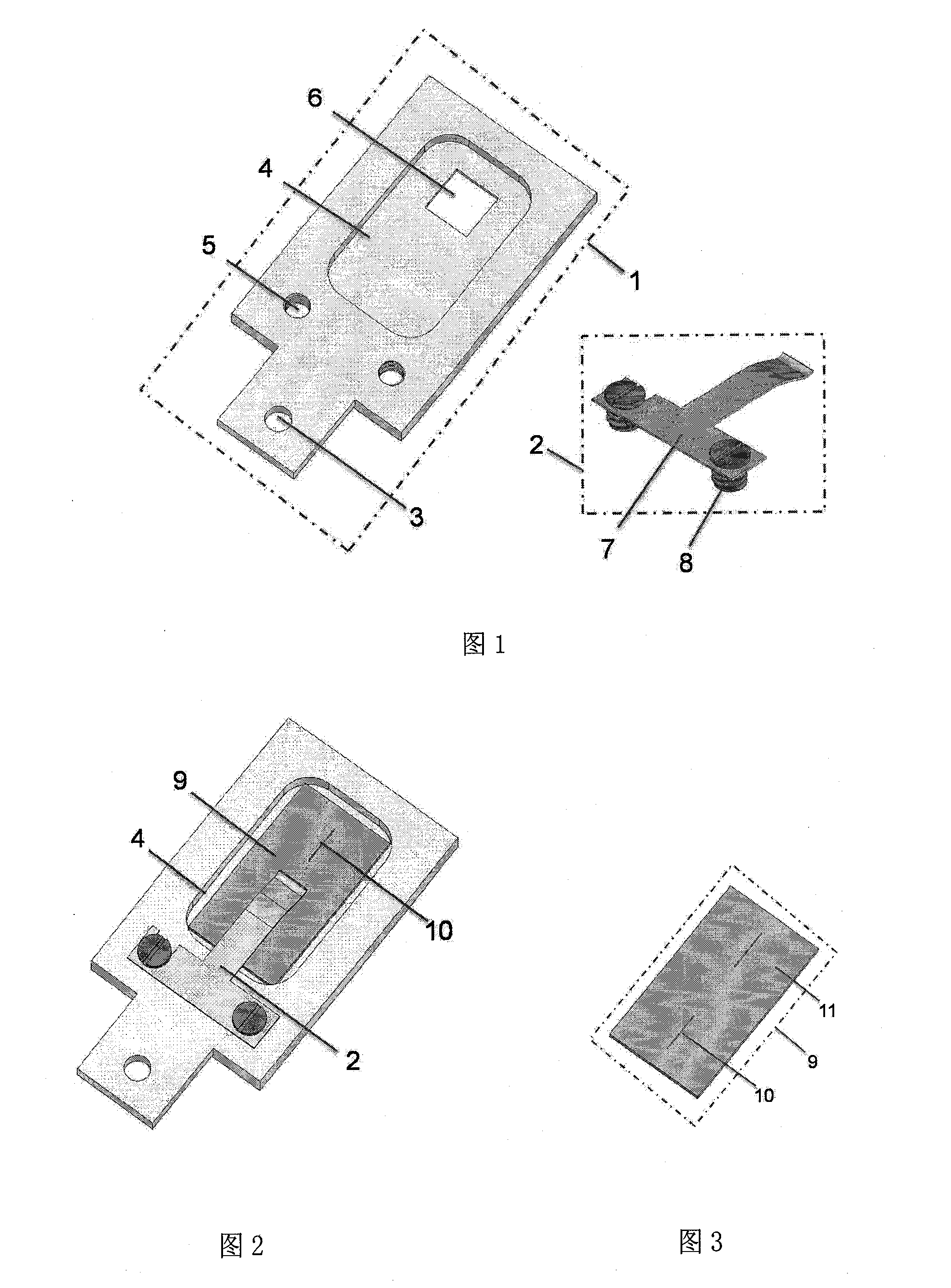
[0029] Referring to accompanying drawing 1, the transmission electron microscope sample stage adapter for property measurement of the present invention comprises preferably plate-shaped adapter body 1 and a fixed substrate component 2 arranged on the adapter body, adapter body 1 One end 3 is matched with the sample stage, the body is provided with a groove 4 and a hole 5 matching with the component 2 for fixing the substrate, a through hole 6 is arranged in the groove 4 close to the other end of the body, and the hole 5 corresponds to the through hole The position is set, preferably at the end opposite to the through hole and close to the end of the adapter body that cooperates with the sample stage. The component 2 for fixing the substrate includes a spring pressing piece 7 and a fixing member 8 (such as a screw, etc.). In a specific embodiment, there is no particul...


PUM

PropertyMeasurementUnit
Depthaaaaaaaaaa
Widthaaaaaaaaaa

Abstract

The invention provides a transmission electronic microscope sample stage connector utilized for property measurement, a substrate for complement use and a production method of the substrate. The invention has the advantages of producing a general TEM sample stage connector by precise mechanical processing and integral semi-conduct process flow, and combining the representing performance of the TEM on the micro structure of the materials and the measuring performance of the material property with the substrate as the carrier. After the substrate finishes the micro structure representation of the TEM, the substrate is taken out and put into any property measuring device which is compatible with the substrate for measuring the mechanics, electronics, optics, thermology, acoustics properties of the materials; meanwhile, a corner of the slit is taken as a mark, thereby guaranteeing the structure representation and the property measurement of the TEM are in the same micro area, which thus can really associate the material micro structure with the properties. In addition, the property measurement can be performed prior to the TEM structure representation.

Description

technical field [0001] The invention belongs to the field of transmission electron microscope accessories, and in particular relates to a transmission electron microscope sample stage adapter used for property measurement, a substrate used in conjunction with it, and a method for manufacturing the substrate. technical background [0002] In recent years, with the deepening of materials science research, especially the rise of nanomaterials science, more and more research results show that the microstructure of materials has a key influence on their properties, so the study of the relationship between the microstructure and properties of materials is of great significance. Significance. As a powerful tool for material structure characterization, transmission electron microscopy can analyze and obtain information such as high-resolution images of materials at the atomic level, electron diffraction patterns, and energy spectra of chemical elements; Microsieves are small in siz...

Claims


Application Information

Patent Timeline
IPC IPC(8): H01J37/20G01N13/10G01N23/04
Inventor 刘开辉白雪冬王恩哥
Owner INST OF PHYSICS - CHINESE ACAD OF SCI
Learn More