
Array substrate of LCD device and its driving method

A technology for liquid crystal display devices and array substrates, applied in static indicators, optics, instruments, etc., can solve the problems of increased cost, increased power consumption, and high overall cost, so as to reduce overall cost, reduce usage, and overcome data lines. The effect of a large number

Inactive Publication Date: 2008-07-16
BOE TECH GRP CO LTD
View PDF0 Cites 64 Cited by
  • Summary
  • Abstract
  • Description
  • Claims
  • Application Information

AI Technical Summary

Problems solved by technology

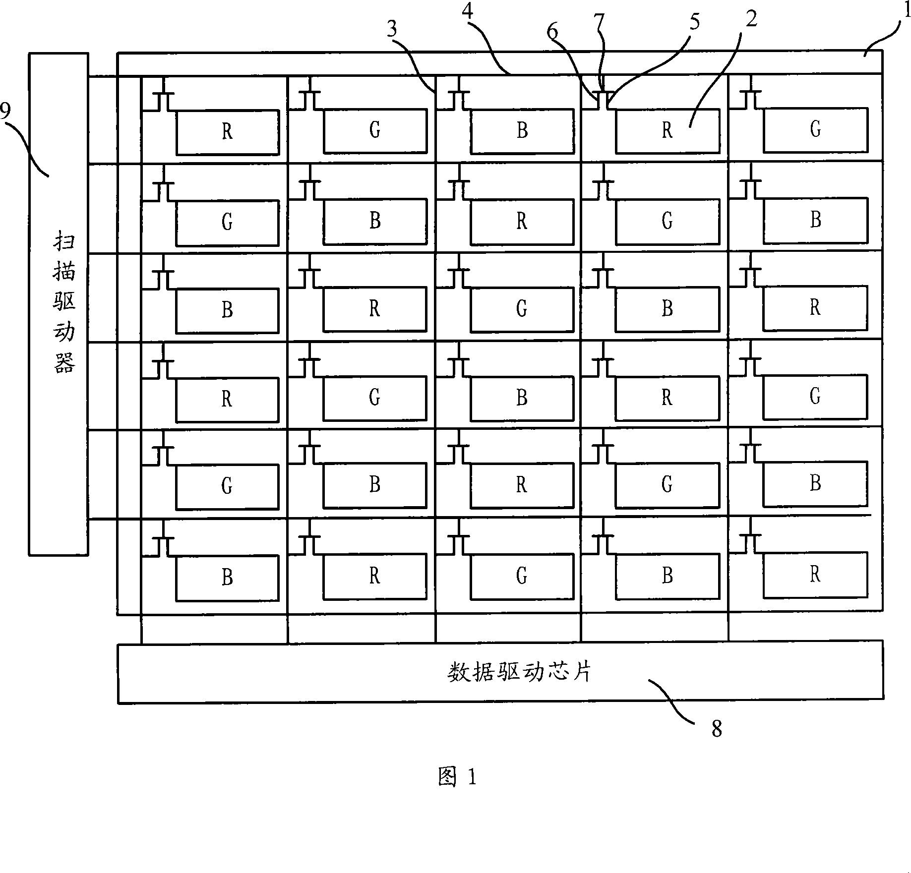
[0004] But the main problem that exists in above-mentioned technology is: first, for TFT-LCD, the driving chip of control driving circuit includes scanning driving chip and data driver, all are indispensable, and the cost of driving chip is lower than TFT-LCD Production costs account for a large proportion, and the data driver chip is more expensive than the scan driver due to its complex structure, making the overall cost of existing TFT-LCD products higher; second, due to the application of R, G, B color filters , which reduces the light transmittance of the liquid crystal display, so a high-brightness backlight is required to achieve a higher display brightness, which will cause a series of problems such as increased cost and increased power consumption.
However, the defect of this technical solution is that due to the increase of white sub-pixels, a corresponding data line needs to be added.
This will cause an increase in the total number of data lines, further causing an increase in the cost of the data driver

Method used


Image

  • Array substrate of LCD device and its driving method
  • Array substrate of LCD device and its driving method
  • Array substrate of LCD device and its driving method

Examples


Embodiment Construction

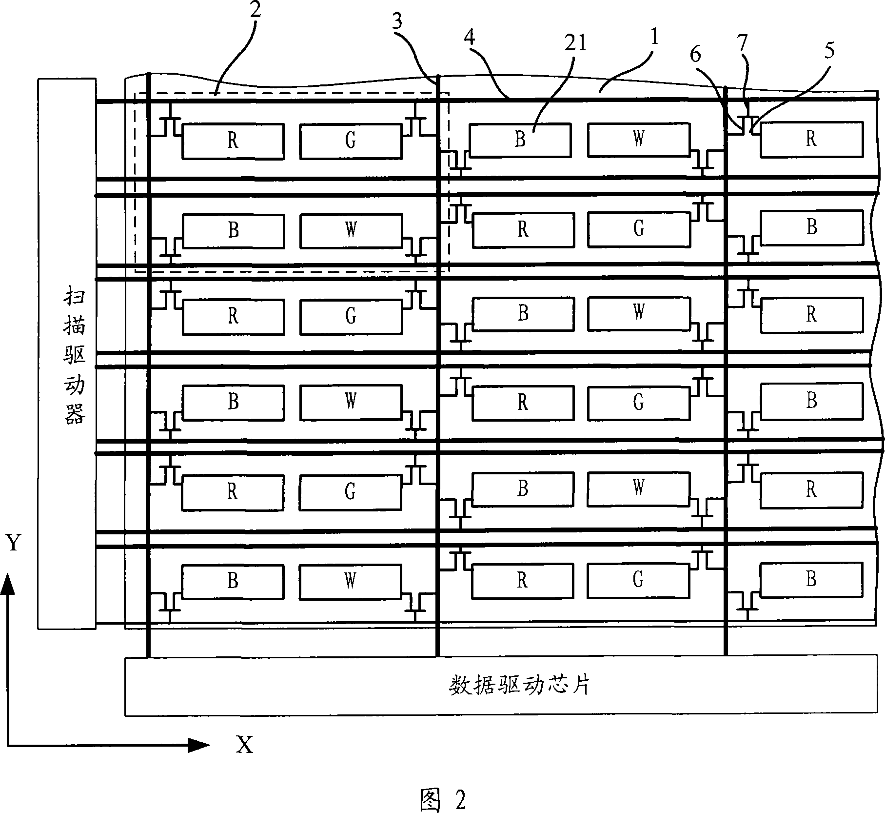
[0022] As shown in Figure 2, it is a structural schematic diagram of Embodiment 1 of the array substrate of the liquid crystal display device of the present invention. The electrode 2 is composed of four sub-pixel electrodes 21 arranged in two rows and two columns. The arrangement of the sub-pixel electrodes 21 is shown in the dotted line box in the figure. Only a few sub-pixels of the array substrate of the liquid crystal display device are shown in FIG. 2 Electrodes 21, wherein the sub-pixel electrodes 21 are arranged on the base substrate 1 in a matrix arrangement, and several parallel data lines 3 are arranged on the base substrate 1 longitudinally, that is, along the Y direction shown in FIG. Parallel scanning lines 4 are arranged on the base substrate 1 laterally, ie along the X direction shown in FIG. 2 . The relative positional relationship of the sub-pixel electrodes 21, the data lines 3 and the scanning lines 4 is specifically: each sub-pixel electrode 21 in the same...


PUM


Abstract

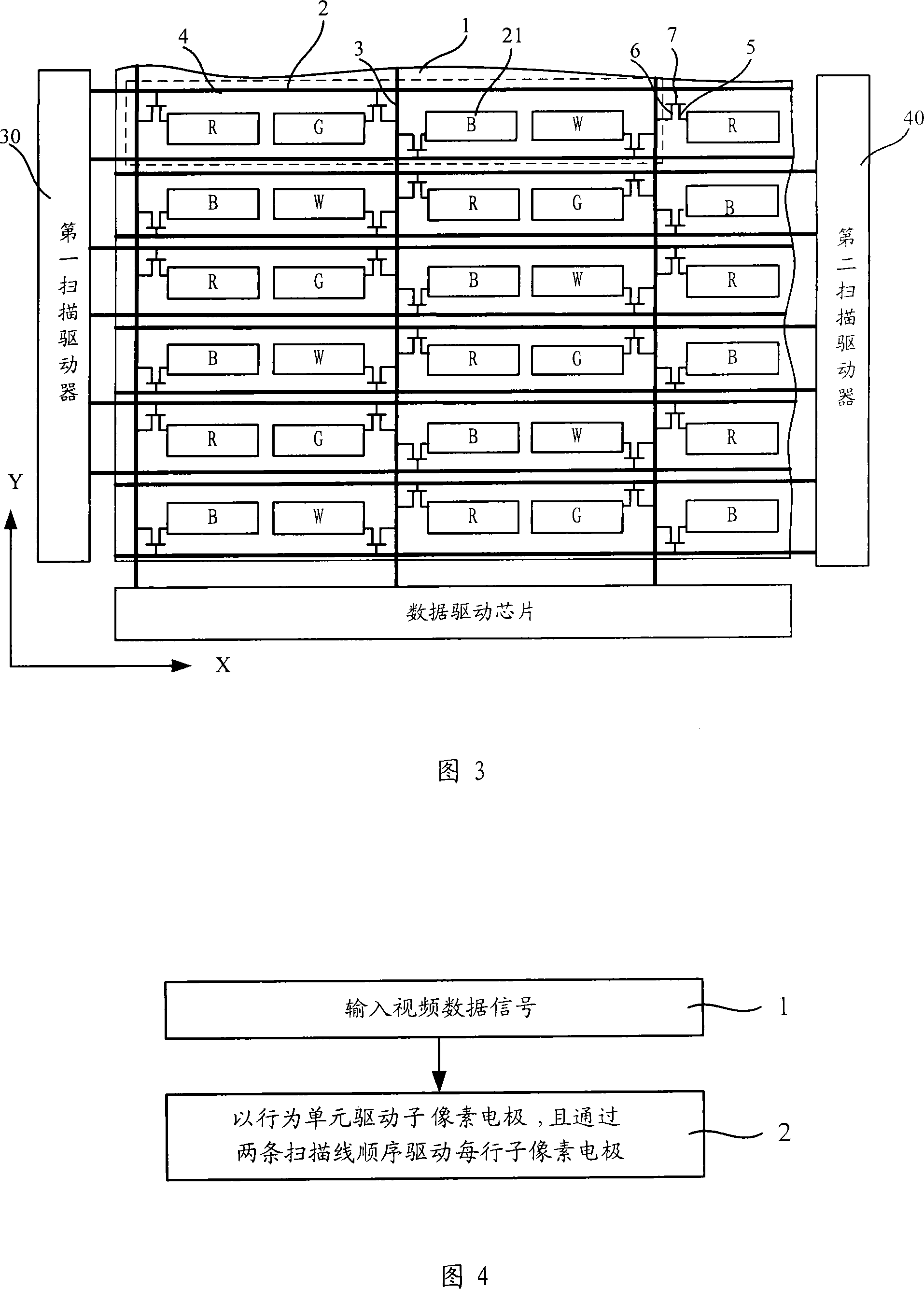
The invention relates to a liquid crystal display array substrate, comprising an underlayer substrate, a plurality of liquid crystal pixel electrodes, data lines and scanning lines, wherein each liquid crystal pixel electrode is composed of four sub-pixel electrodes, and the sub-pixel electrodes in the same column are connected to the same data line. Each data line is connected with two columns of sub-pixel electrodes; the pixel electrodes in the same row are respectively and alternatively connected with two scanning lines, with each two as a group. The sub-pixel electrodes connected with each scanning line are in the same row; two sub-pixel electrodes in the same line between two adjacent data lines are connected with the same scanning line and are respectively connected with the two data lines as well. The invention also relates to a method for driving the same liquid crystal display array substrate. The invention adopts a means that the sub-pixel electrodes in the same row are driven by double scanning lines, and two columns use one data line, which reduces data lines needed, used data drive chips and total cost of the liquid crystal display.

Description

technical field [0001] The present invention relates to an array substrate of a liquid crystal display device and a driving method, in particular to an array substrate of a thin-film transistor liquid crystal display device including four sub-pixels of R, G, B and W and a driving circuit on the array substrate. method. Background technique [0002] Thin Film Transistor-Liquid Crystal Display (Thin Film Transistor-Liquid Crystal Display, hereinafter referred to as TFT-LCD) is one of the most widely used flat panel displays at present. TFT-LCD generally includes a liquid crystal display panel, a scan drive circuit and a data drive circuit. Wherein, the liquid crystal display panel includes a color filter substrate and a TFT array substrate arranged in opposite boxes, and a liquid crystal layer sandwiched between the two substrates, and a scanning driving circuit and a data driving circuit are respectively connected to the TFT switching elements on the array substrate. As sho...

Claims


Application Information

Patent Timeline
Patent Type & Authority Applications(China)
IPC IPC(8): G02F1/1362G09G3/36H01L27/12
Inventor 邵喜斌尹海军张俊瑞
Owner BOE TECH GRP CO LTD
Learn More